Optical Spacers: The Silent Enablers in Next-Gen Optoelectronics—Market to Reach $447 Million by 2032
In the ever-evolving world of optoelectronics and photonics, the optical spacer—an unassuming, ultra-thin layer often invisible to the naked eye—is quietly driving some of the most significant technological advances of the decade. Once viewed as a simple physical buffer or alignment aid, today’s optical spacers have transformed into highly engineered, multifunctional components critical to everything from solar power and smartphones to LiDAR systems and micro-optics packaging.
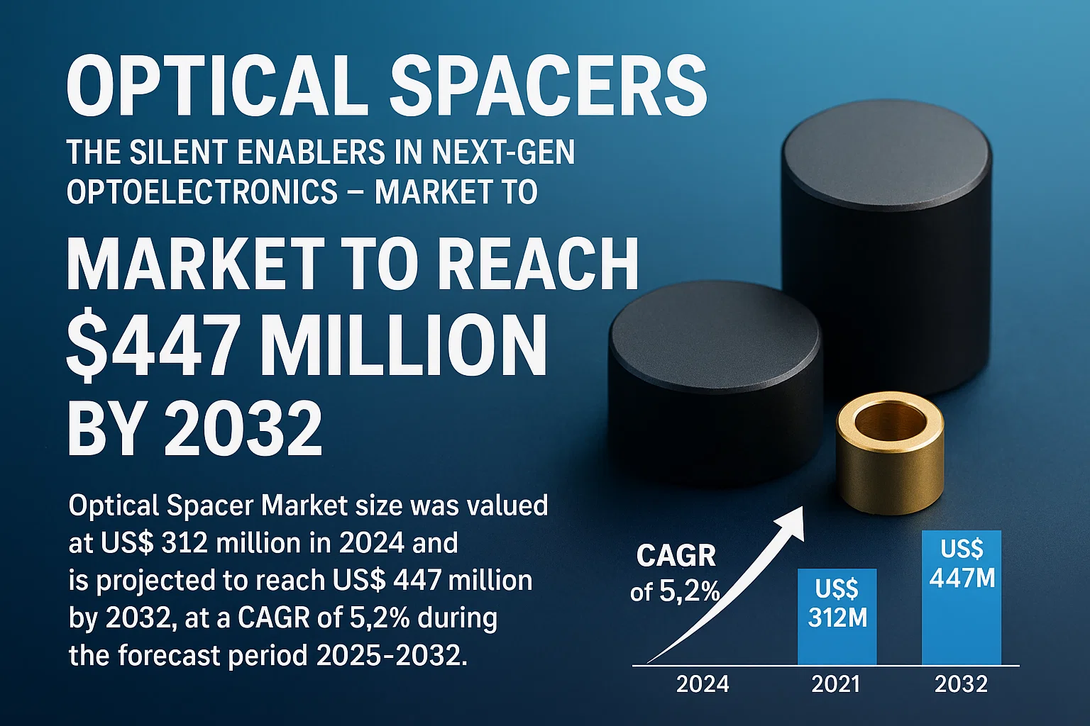
According to recent data, the Optical Spacer Market was valued at US$ 312 million in 2024 and is projected to grow to US$ 447 million by 2032, expanding at a CAGR of 5.2% during the 2025–2032 forecast period. This growth reflects not just increasing demand but a fundamental rethinking of what optical spacers can do—and how they’re made.
From Passive Filler to Precision Enabler
A decade ago, optical spacers were largely confined to the role of mechanical separators—plastic or glass shims used in lenses or displays. But the industry is rapidly moving past that. Spacers are now being used to optimize optical paths, reduce reflectivity, improve thermal stability, and even serve as temporary fixtures in advanced manufacturing.
Recent developments underscore this shift:
- Qcells recently set a new lab record for perovskite-silicon tandem solar cell efficiency (28.6%), thanks in part to a nano-textured optical spacer that balances light absorption between the two layers. Such innovation is paving the way for commercial tandem modules by 2026.
- In the smartphone camera space, researchers at the University of Tokyo and JSR Corporation are replacing traditional multi-component spacer-lens systems with a flat, micro-patterned Fresnel lens layer that doubles as an optical spacer. This advancement could significantly reduce module thickness, a crucial win for compact electronics.
- Kyocera’s new LiDAR-camera fusion sensors integrate a moulded optical spacer that aligns both sensor axes with extreme precision. This alignment solves the parallax issues that have long plagued dual-sensor systems, especially in autonomous vehicles and advanced driver-assistance systems (ADAS).
Optical Spacers in Display Technology: Clear Gains
Displays, particularly those used in outdoor, rugged, or medical environments, are also reaping the benefits of spacer innovation. Kyocera Display has adopted a vacuum optical bonding process that eliminates traditional acrylic tape spacers and uses flowable optically clear adhesives (OCAs) instead. This approach reduces internal reflections from 13.5% to 0.2%, offering clearer, more sunlight-readable screens.
The move toward zero-gap bonding isn’t just an aesthetic upgrade—it enhances durability, reduces condensation risk, and boosts optical performance across multiple sectors.
Semiconductor Packaging and Spacer Convergence
Optical spacer technology is also crossing over into semiconductor packaging. DELO, a German material innovator, recently showcased a UV-curable mould compound that acts as both a spacer and a temporary alignment fixture in wafer-level MEMS packaging. After reflow, the spacer dissolves cleanly under UV light, preserving precision and eliminating waste.
This blurring of lines between optical engineering and advanced packaging signals a broader trend: integrated functionality is becoming the norm.
Regional Realignment and Supply Chain Strategy
With geopolitical and economic pressures reshaping global supply chains, optical spacer manufacturers are adjusting accordingly. LightPath Technologies, for instance, recently opened a new coating facility in Latvia, which features an integrated sol-gel optical spacer within its anti-reflective coatings. This allows for faster, more resilient production of IR optics—especially important for European aerospace and defense sectors that seek to reduce reliance on foreign-sourced germanium.
What’s Driving Market Growth?
Several factors are converging to fuel demand for advanced optical spacer solutions:
- Miniaturization of optical systems in mobile devices and wearables
- Efficiency demands in renewable energy systems, especially tandem solar cells
- Sensor fusion in autonomous vehicles, where optical precision is mission-critical
- Increased ruggedization of displays for industrial, medical, and military applications
- Push for localized, integrated manufacturing amid global supply chain shifts
Smart and Adaptive Spacers?
The next chapter in optical spacer innovation could be adaptive materials—photo-reflow polymers or phase-change compounds that allow for post-assembly cavity tuning, aberration correction, or light filtering. These would not only simplify design and reduce part counts but could also unlock dynamic calibration in real time for devices like AR glasses or head-up displays.
In a world that obsesses over sensors, lenses, and processors, optical spacers remain the unsung heroes—but their time in the spotlight is drawing near. As their roles evolve from structural support to optical tuning, alignment, and even smart integration, the market for these tiny but transformative components is poised for robust growth.
By 2032, the optical spacer won’t just be something you sandwich between components—it’ll be a key enabler of everything from clean energy to machine vision.
Comments (0)