
NY CREATES Joins 12-Inch Mask Initiative as Advanced Materials Become Critical to High-NA EUV Scaling
The semiconductor industry is moving into a phase where lithography progress is no longer being measured only by how small a feature can be printed, but also by how efficiently increasingly complex chips can be manufactured. Against this backdrop, NY Creates has announced its participation in a new 12-inch mask industry initiative aimed at strengthening the ecosystem required for High Numerical Aperture Extreme Ultraviolet (High-NA EUV) lithography.
The collaboration brings together semiconductor industry stakeholders to address one of the emerging challenges surrounding High-NA EUV adoption: the limitations of conventional EUV mask dimensions when manufacturers need to produce increasingly large and complex chip designs at advanced process nodes.
- Conventional EUV lithography uses reticles measuring approximately 6-by-6 inches. While this format has supported leading-edge semiconductor manufacturing, High-NA EUV introduces a different set of optical and manufacturing considerations.
- High-NA systems are designed to deliver substantially higher imaging resolution, enabling semiconductor manufacturers to pursue increasingly advanced technology nodes. However, the higher numerical aperture also reduces the field size that can be exposed in a single shot.
- For large chip designs, this can create a need to divide patterns across multiple exposures and subsequently stitch them together. While this approach can enable larger structures to be manufactured, it introduces additional process complexity and can place greater pressure on productivity, overlay accuracy and yield.
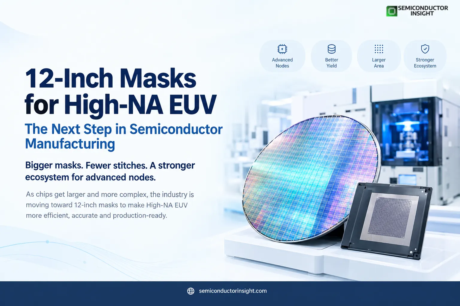
- The industry is therefore exploring a 6-by-12-inch mask format, commonly referred to as a 12-inch mask, to increase the printable area available during exposure.
- If successfully developed and industrialized, the larger mask format could help reduce stitching requirements for larger dies while improving the practicality of High-NA EUV for future high-volume manufacturing environments.
NY Creates’ participation comes as the organization prepares to expand its High-NA EUV capabilities through its High-NA EUV Lithography Center at the Albany NanoTech Complex.
The initiative is particularly significant because High-NA EUV adoption requires much more than installing advanced lithography equipment. A functioning manufacturing ecosystem must also support the development and qualification of critical components surrounding the exposure process.
This includes:
- Advanced mask blanks
- Mask-writing technologies
- Mask inspection systems
- High-performance pellicles
- Reticle handling and transportation systems
- Mask manufacturing infrastructure
- Process integration and metrology capabilities
NY Creates’ position as a collaborative semiconductor R&D hub provides an environment in which equipment suppliers, chipmakers, research organizations and other ecosystem participants can work on these challenges collectively.
The initiative also aligns with NY Creates’ partnership ecosystem and its work involving ASML’s High-NA EUV technology.
High-NA EUV is widely viewed as one of the key technologies supporting the industry’s continued scaling toward extremely advanced semiconductor architectures. Its ability to provide higher-resolution imaging is expected to become increasingly important as chipmakers develop smaller features and more sophisticated device structures.
The technology is particularly relevant to applications driven by rapidly increasing computational requirements, including artificial intelligence, high-performance computing, advanced data centers and next-generation processors.
However, the commercial impact of High-NA EUV will ultimately depend on whether the broader manufacturing ecosystem can keep pace with the lithography platform itself.
Collaboration Becomes the Next Scaling Lever
The 12-inch mask initiative highlights a broader transformation taking place across semiconductor manufacturing: advanced-node scaling is increasingly becoming an ecosystem challenge rather than a single-equipment challenge.
As process technologies become more sophisticated, improvements in lithography must be supported by coordinated advances in masks, materials, inspection, metrology, process control and manufacturing infrastructure.
NY Creates is participating alongside industry stakeholders including ASML, TSMC and other partners, creating a collaborative environment focused on addressing these challenges before the technology needs to move into high-volume manufacturing.
This collaborative model could become increasingly important as semiconductor manufacturers attempt to balance aggressive node scaling with manufacturing economics, yield and production efficiency.
The larger message is clear: the next phase of semiconductor scaling will depend not only on shrinking features, but on redesigning the infrastructure that makes advanced lithography commercially practical.
With NY Creates joining the 12-inch mask initiative, industry collaboration is gaining another important platform as semiconductor manufacturers prepare for the increasingly demanding requirements of High-NA EUV and future leading-edge nodes.
Don’t Forget to Surf Our Updated Report for More Detailed Analysis: https://semiconductorinsight.com/report/ai-assisted-euv-stochastics-defect-prediction-market/

Comments (0)