Nikon Enters CMP Market with New 200 mm Platform to Support Legacy Fab Growth
In the evolving landscape of semiconductor manufacturing, the role of Chemical Mechanical Polishing (CMP) is paramount. While the industry often directs its spotlight toward the more glamorous 300 mm wafer technologies and cutting-edge EUV lithography, 200 mm wafers continue to be the unsung heroes, particularly in sectors like power devices, analog ICs, and MEMS.
According to recent data, the 200 mm Wafer CMP Machines market was valued at USD 452 million in 2024. It is projected to grow at a CAGR of 4.7%, reaching USD 619 million by 2032.
The Market Landscape: Why 200 mm Still Matters
Even as the semiconductor industry shifts toward advanced nodes and larger wafer diameters, 200 mm wafers remain vital for high-volume, cost-effective production of mature-node chips. Industries relying on these include:
- Automotive electronics (EVs, inverters, motor control ICs)
- IoT and wearable devices
- MEMS sensors and RF chips
- Silicon Carbide (SiC) and Gallium Nitride (GaN) power devices
These application areas rarely require the high-density integration offered by 300 mm wafers. What they demand instead is manufacturing reliability, mature process control, and cost-efficiency—features well served by 200 mm CMP systems.
What Is Chemical Mechanical Polishing?
CMP is a planarization technique that combines chemical etching and mechanical abrasion to smooth semiconductor surfaces during wafer processing. It’s essential for:
- Dielectric planarization
- Copper interconnect formation
- Wafer-level packaging
- SiC and GaN polishing
CMP is the final polishing step to remove topographic variations from previous deposition and etching steps. In 200 mm fabs, this process is increasingly optimized for new substrates like SiC, as well as for legacy silicon wafers used in automotive-grade chips.
Market Forecast: 2024 to 2032
- 2024 Market Size: USD 452 million
- Projected 2032 Market Size: USD 619 million
- CAGR: 4.7%
This growth is being propelled by several overlapping trends:
- Expansion of electric vehicle (EV) production
- Increased deployment of IoT devices
- Surging demand for wide bandgap semiconductors
- Sustained investment in mature-node foundries across Asia and Europe
Additionally, many global chipmakers are upgrading their 150 mm lines to 200 mm capacity, which drives demand for new-generation CMP tools compatible with legacy fab footprints.
Recent Developments Reshaping the Industry
- Applied Materials Launches Mirra Durum CMP System for SiC Wafers
One of the most significant developments in recent years is Applied Materials’ release of the Mirra Durum CMP tool, targeted at 200 mm SiC wafer processing. Launched alongside the VIISta 900 hot ion implant system, this CMP platform enables:
- Support for 200 mm SiC wafers
- Improved removal rate control for hard materials
- Reduction of total cost of ownership via efficient slurry use
Why it matters: As EV powertrain inverters and fast-charging solutions increasingly rely on SiC technology, the Mirra Durum offers fab engineers a pathway to scale up without transitioning to a 300 mm line.
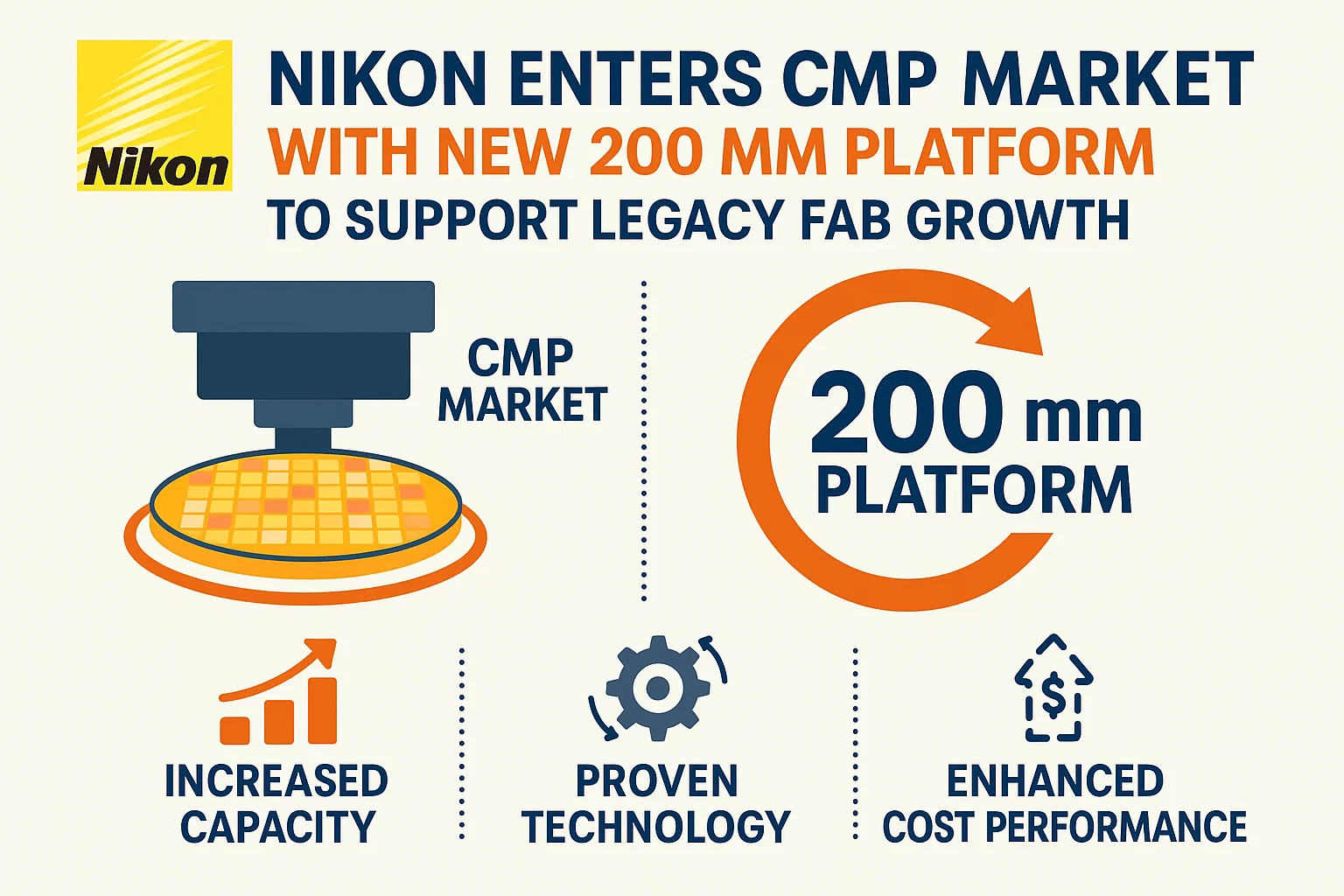
- Nikon’s Entrance into CMP with the NPS2301 System
In an unexpected move, Nikon—long known for lithography and metrology tools—entered the CMP market with its NPS2301 platform in 2024. Co-developed with Okamoto Machine Tool, this tool is optimized for:
- Copper/low-k dielectric planarization
- 150 mm to 200 mm wafer compatibility
- Reduced slurry consumption (up to 25%)
- 50 wafers-per-hour throughput
Though its primary target is 150 mm fabs, Nikon has confirmed that a 200 mm variant is under testing, with early evaluations from Japanese analog and MEMS fabs underway.
- Academic Research on Polishing SiC and GaN Wafers
While CMP for silicon wafers is a mature field, the polishing of hard substrates like SiC and GaN at 200 mm scale is still evolving. Recent papers from the University of Tokyo and Indian Institute of Science (Bangalore) highlight:
- The use of colloidal silica with modified abrasive size distribution
- The effect of oxidizing agents like H2O2 in slurry formulations
- Optimization of pad grooving and conditioning cycles
These innovations are enabling faster planarization with lower defectivity, an essential step for meeting automotive and power semiconductor standards.
Key Market Segments
- By Application
| Application Area | Market Share (%) | Comments |
| Power Semiconductors | 34% | Driven by SiC/GaN transition in EV infrastructure |
| MEMS and Sensors | 22% | High-volume production needs smooth topography |
| Analog/RF Devices | 20% | Critical for 5G and satellite systems |
| Discrete Components | 14% | MOSFETs, IGBTs for industrial and telecom use |
| Others (LEDs, etc.) | 10% | Emerging categories leveraging 200 mm lines |
- By Region
- Asia-Pacific: Dominates the market (~50%), with Japan, China, and Taiwan leading fab expansions.
- North America: Focus on legacy fab upgrades and automotive-grade chip development.
- Europe: Investments from STMicroelectronics and Infineon to localize SiC production.
- Rest of World: Rising interest from India, Israel, and Southeast Asia.
Key Players in the 200 mm CMP Market
| Company | Notable Product/Service |
| Applied Materials | Mirra Durum CMP for 200 mm SiC wafers |
| Nikon | NPS2301 CMP system for 150/200 mm copper polishing |
| Ebara Corporation | Slurry delivery and CMP platforms for MEMS fabs |
| Revasum | 7AF-HMG polisher (high-performance SiC CMP) |
| Lapmaster Wolters | Double-sided polishing systems for compound semis |
| Okamoto | Partnered with Nikon; strong in legacy wafer polish |
Innovation in Slurry and Pad Technologies
Pad Innovations
Modern CMP machines increasingly rely on engineered pads with advanced grooving to improve slurry distribution and reduce wafer scratching. Some trends include:
- Hard pads with laser-cut micro-grooves
- Advanced conditioning disks with AI-optimized dressing patterns
- Hybrid pads that reduce pad wear while boosting removal rates
Slurry Optimization
- Adoption of slurry-on-demand delivery systems to cut waste
- Increasing use of nanoparticle abrasives for ultra-smooth SiC surfaces
- Customized pH and oxidizer combinations for GaN, SiGe polishing
These innovations are especially relevant for 200 mm CMP, where cost sensitivity and sustainability are paramount.
Challenges Hindering Market Expansion
Despite the market’s solid growth trajectory, a few barriers remain:
- High Cost of CMP Consumables
Slurries, conditioners, and pads often represent 30–40% of total CMP cost per wafer. - SiC Wafer Fragility and Variability
Unlike silicon, SiC wafers are prone to chipping and fracture, making polishing more delicate. - Global Supply Chain Disruption
Shortages of slurry chemicals and polishing pads due to geopolitical tensions have led fabs to seek localized sources. - Tool Obsolescence in Legacy Fabs
Many 200 mm fabs still operate on outdated CMP tools, requiring either costly retrofitting or full tool replacement.
Future Outlook: What’s Next?
- Retrofitting 200 mm CMP Tools for Advanced Substrates
Expect to see increased tool upgrades rather than full replacements—enabling fabs to handle SiC/GaN without overhauling their production lines.
- AI-Driven CMP Process Control
Startups and research labs are working on real-time endpoint detection using machine learning, optimizing polish uniformity and defect control.
- Localized Manufacturing of CMP Consumables
With geopolitical concerns and environmental pressure, regions like India and the EU are investing in domestic slurry and pad production.
- Sustainable CMP Practices
Waste slurry recycling, reduced water usage, and biodegradable pad materials are now part of ESG goals for semiconductor manufacturers.
The 200 mm Wafer Chemical Mechanical Polishing Machines Market may not grab the same headlines as EUV lithography or 3D NAND stacking—but it remains a vital segment that’s growing steadily in both value and sophistication.
With a projected CAGR of 4.7% and a forecasted market size of USD 619 million by 2032, it’s clear that 200 mm CMP is far from obsolete. It is, in fact, adapting, innovating, and thriving—playing a crucial role in supporting legacy applications, new power devices, and cost-efficient chipmaking across the globe.
As the world demands smarter, greener, and more connected devices, 200 mm CMP technology is quietly enabling that future, one polished wafer at a time.
Comments (0)