Naura, AMEC, and SiCarrier Shake Up Global Etch Equipment Market Amid China’s Tech Rise
The semiconductor industry is undergoing a profound transformation, driven by surging demand for advanced nodes, AI workloads, edge computing, and green technologies. At the heart of this revolution lies one of the most critical yet often overlooked segments—Wafer Used Dry Etching Equipment. With the market valued at US$ 9.67 billion in 2024 and projected to soar to US$ 18.42 billion by 2032, this sector is growing at an impressive CAGR of 9.7% during the 2025–2032 forecast period. Behind this growth are cutting-edge innovations, fierce geopolitical competition, and rising demand for sustainability in chip fabrication.
Access Your Free Sample Report- Wafer Used Dry Etching Equipment Market
What is Wafer Dry Etching—and Why It Matters
Dry etching is a plasma-based process used to precisely remove material from a wafer during semiconductor manufacturing. Unlike wet etching, which uses liquid chemicals, dry etching relies on ionized gases (plasmas) to carve fine patterns on the wafer’s surface. It’s particularly vital for fabricating advanced-node chips where dimensional precision and aspect ratio control are essential—making it a cornerstone in the production of DRAM, NAND, and cutting-edge logic chips at sub-5nm nodes.
The significance of dry etching has grown exponentially due to the rise of 3D architectures, such as FinFET and 3D NAND, which require ultra-precise etch control to ensure functionality, performance, and yield.
Market Outlook: 2024–2032 Growth Drivers
The global Wafer Used Dry Etching Equipment Market is expected to grow from US$ 9.67 billion in 2024 to US$ 18.42 billion by 2032, at a CAGR of 9.7%. Several key drivers are propelling this expansion:
1. Advanced Node Transition
With chipmakers moving toward 3nm and beyond, the demand for atomic-level etching has surged. Technologies like Atomic Layer Etching (ALE) and High Aspect Ratio Contact (HARC) etching are becoming standard.
2. Proliferation of AI & HPC
AI accelerators, high-performance computing (HPC), and 5G infrastructure demand chips with extremely tight feature tolerances. This necessitates advanced dry etch tools with real-time process control and AI-driven endpoint detection.
3. 3D NAND and DRAM Scaling
The memory industry continues to push toward higher layers in 3D NAND (currently over 232 layers). These vertical stacks require deep and narrow etch profiles, boosting the demand for specialized dry etch systems.
4. Emerging Geopolitical and Localization Pressures
Countries like China are racing to develop indigenous semiconductor capabilities. Investments in domestic dry etch tool production are accelerating, adding new competitive dynamics to the global market.
Recent Global Developments Driving Change
The following section dives deep into recent news and strategic shifts that are shaping the market dynamics.
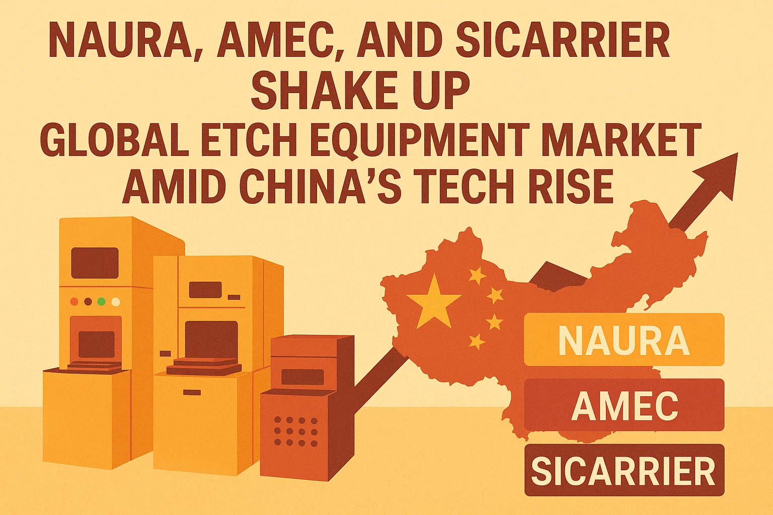
China’s Etching Push: Naura, AMEC & SiCarrier Making Headlines
Naura and AMEC’s Explosive Growth
According to Reuters, China’s top equipment makers—Naura Technology Group and Advanced Micro-Fabrication Equipment Inc. (AMEC)—have seen dramatic revenue surges in 2024. Naura’s revenue grew nearly fivefold to ¥29.8 billion, while AMEC quadrupled its earnings to ¥9.1 billion. These companies are focusing on dry etch, CVD, and other critical wafer processes.
“Domestic leaders like AMEC are making fast progress in etch tools used in NAND and DRAM,” noted a Tsinghua-affiliated analyst.
(Source: Reuters, May 2025)
While most of their equipment currently serves mature nodes (28nm and above), they are increasingly targeting nodes below 14nm—a significant leap in technical sophistication.
SiCarrier: Huawei’s Ally in Lithography and Etch
In another development, SiCarrier, a Huawei-affiliated firm, raised $2.8 billion at a $11 billion valuation to develop a full suite of chipmaking tools—including dry etchers. Though many of its tools remain pre-commercial, its close ties to Huawei and aggressive funding have placed it on the radar of global competitors.
At SEMICON China 2025, SiCarrier unveiled over 30 new semiconductor tools—including etching machines—despite skepticism over their readiness for production-level integration.
Challenge Ahead: Advanced Node Capability
Despite these advancements, China’s domestic etch tools are still far from self-sufficiency for advanced nodes (<7nm). Global market leaders remain dominant in the cutting-edge space, especially for 3nm and gate-all-around (GAA) architectures.
Global Innovation: Lam Research, TEL, and Applied Materials Maintain Edge
Leading global players continue to innovate aggressively to maintain their advantage.
Lam Research
Lam is pushing the boundaries in Atomic Layer Etching (ALE) and High Aspect Ratio Etch (HARC)—both essential for 3D NAND and FinFETs. Its Sense.i platform leverages AI for real-time process control, improving yield and reducing downtime.
Tokyo Electron (TEL)
TEL is expanding its etch and deposition solutions with an emphasis on multi-patterning, ultra-thin film etching, and low-damage processing—key for sensitive DRAM and logic nodes.
Applied Materials
Applied is investing heavily in eco-efficient etch systems that cut energy use and process gas emissions. Its Centura platform has been updated to support next-gen node scaling, combining etch with advanced metrology for tighter process windows.
Download Sample Report PDF- Wafer Used Dry Etching Equipment Market
Sustainability Is the New Standard
The environmental impact of semiconductor manufacturing is coming under increasing scrutiny. Dry etching equipment—especially those using fluorinated gases (F-GHGs)—contributes significantly to fab emissions.
Emerging Green Innovations:
- Closed-Loop Gas Recycling: Several toolmakers are introducing systems that recycle plasma gases, reducing emissions by up to 45%.
- Energy-Efficient Plasma Chambers: New chamber designs reduce power consumption by 30–40%, without sacrificing etch precision.
- Modular Upgrades: Instead of full replacement, modular upgrades to older etch systems reduce e-waste and extend tool lifespans.
These eco-innovations are becoming key differentiators as fabs aim for net-zero emissions by 2030 and beyond.
AI, Automation, and Smart Etching
The integration of AI-driven diagnostics, real-time sensors, and automated chamber tuning is transforming dry etching into a smart, adaptive process.
Key Capabilities:
- AI Endpoint Detection: Reduces scrap rates by accurately determining when etching is complete.
- Predictive Maintenance: Sensors and AI models forecast tool failure before it happens.
- Digital Twins: Simulated models of etch chambers allow for remote process testing and optimization.
These technologies are especially vital for foundries operating at sub-5nm, where even slight deviations can lead to catastrophic yield losses.
Competitive Landscape Snapshot (2025–2032)
| Company | Focus | Notable Advantage |
| Lam Research | ALE, 3D NAND, AI tools | Strong AI + sustainable process design |
| Tokyo Electron | High precision logic etch | Advanced multi-patterning etch |
| Applied Materials | Green etch platforms | Integrated metrology + etch systems |
| Naura (China) | Memory & legacy nodes | Domestic market dominance |
| AMEC (China) | Etch for DRAM/NAND | Fast scaling in China’s 28–14nm fabs |
| SiCarrier (China) | Full-stack litho + etch | Strong Huawei link + deep funding |
End-User Trends: What Fabricators Want
Semiconductor fabs are evolving into ultra-automated, environmentally conscious, and AI-integrated ecosystems. Here’s what end-users are prioritizing when selecting dry etch systems:
- Tool Flexibility: Single chamber able to support multiple etch chemistries and wafer types.
- Yield Optimization: AI-integrated process control to reduce scrap rates and tool downtime.
- Cost of Ownership (CoO): Low-maintenance design, high uptime, and upgradeability.
- Sustainability Compliance: Green certifications and compatibility with ESG goals.
Foundries like TSMC, Samsung, and Intel are now requiring strict carbon accounting and GHG limits across equipment suppliers.
Future Trends and Forecast: 2025–2032
1. Sub-3nm Process Integration
As the industry enters GAA-FET and nanosheet territory, the complexity of etch requirements will increase exponentially.
2. EUV Synergy with Etch
Etch will increasingly integrate with EUV lithography, particularly in double patterning and spacer-defined processes.
3. China’s Technology Leap?
Though lagging at advanced nodes, expect China to achieve partial parity at 14nm and 10nm by 2030, fueled by national funding and R&D incentives.
4. Etch-as-a-Service?
With fabless companies and startups entering the chip space, equipment-as-a-service (EaaS) models may emerge, offering etching capabilities through shared facilities.
Click Here To Download Full Sample Report- Wafer Used Dry Etching Equipment Market
The Wafer Used Dry Etching Equipment Market is entering a golden era, fueled by the convergence of technology transitions, sustainability mandates, and geopolitical imperatives. With a projected value of US$ 18.42 billion by 2032, the industry is primed for innovation, disruption, and strategic realignment.
Whether it’s AI-enabled process control, carbon-neutral etching, or China’s aggressive manufacturing ambitions, dry etch tools will be central to the future of semiconductor manufacturing.
In this race for precision, performance, and sustainability, those who innovate faster—and greener—will define the next generation of silicon.
Comments (0)