
Mask Blanks Market: Reflective vs. Transmissive Architectures
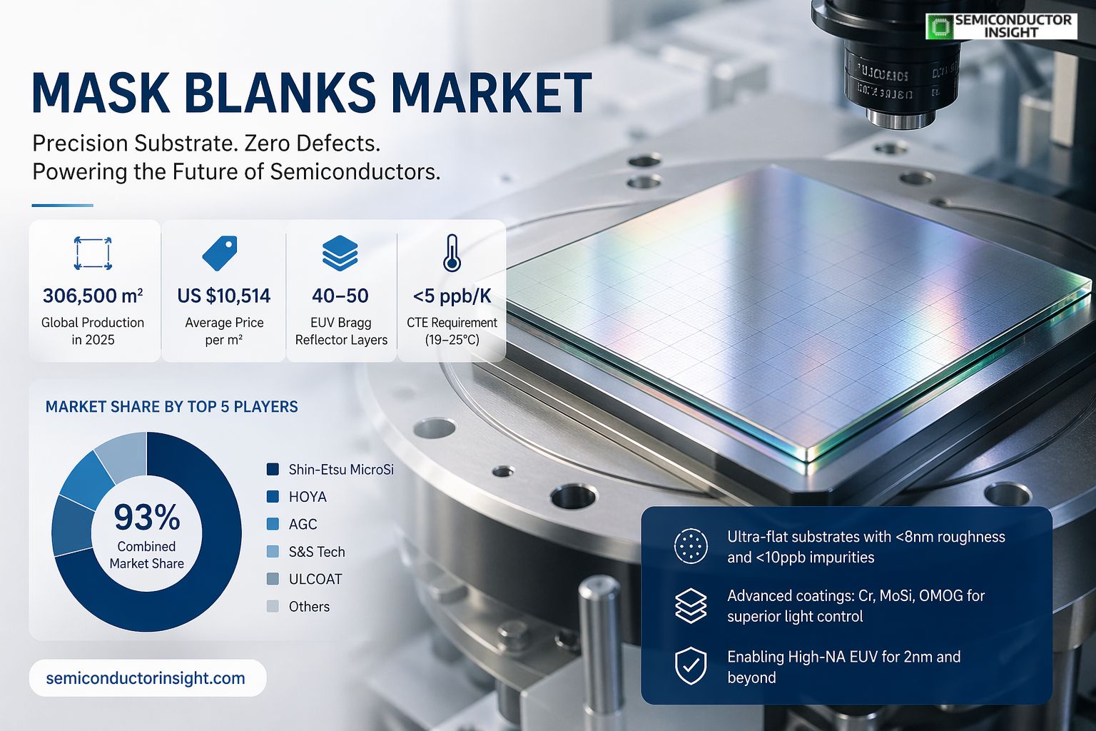
The industrial capacity for manufacturing mask blanks is directly tethered to the global demand for logic and memory chips. Unlike typical consumer goods, the volume here is measured not in units but in square meters of ultra-flat substrate real estate. In 2025, the worldwide physical production of photomask substrates (commonly referred to as mask blanks) was recorded at 306,500 square meters.
To contextualize this industrial output, the average pricing per square meter stood at approximately US $10,514. This high valuation per unit area is justified by the extreme technical requirements; a single defect on a mask blank can render an entire batch of high-performance computing chips defective. The market operates on a binary logic of zero defects for leading-edge nodes, making physical yield management the primary value driver rather than sheer volume.
EUVL Infrastructure: The 40-Layer Bragg Reflector
- Transitioning to extreme ultraviolet lithography (EUVL) necessitates a fundamental redesign of the mask blank architecture.
- For nodes at 7nm and below, the industry cannot use traditional transmissive quartz blanks because EUV light (13.5nm wavelength) is absorbed by virtually all materials.
- Instead, Mask Blanks Market supplies reflective mask blanks. These are not simple coated plates but complex distributed Bragg reflectors.
- Current manufacturing specifications require the deposition of alternating 40 to 50 layers of molybdenum and silicon on a defect-free substrate.
- Each layer pair must maintain strict periodicity to achieve the required reflectivity of approximately 60-70% at normal incidence.
- The total thickness of this stack is controlled within a few nanometres across a 150mm x 150mm surface.
- In order to prevent thermal stress from warping the blank during the powerful synchrotron radiation in an ASML scanner, suppliers have to innovate beyond normal deposition to atomic layer precision.
Material Science Metrics: Coefficient of Thermal Expansion (CTE)
The physical stability of the substrate material is the single most critical parameter for mask blanks used in high-energy lithography. Industry specifications, such as the SEMI Standard P37, mandate that mask blanks exhibit an extreme low thermal expansion profile. For advanced nodes, the required CTE is less than 5 parts per billion per Kelvin (ppb/K) across the operating temperature range of 19 to 25 degrees Celsius.
To achieve this, manufacturers utilize specialized glass-ceramics and titanium-silicate glasses. Corning’s ULE (Ultra Low Expansion) glass, composed of a binary SiO2-TiO2 mixture, is processed to eliminate compositional striae, achieving mid-spatial frequency roughness of less than 8 nanometres peak-to-valley. This accounts for less than 20% of the total 50nm flatness error budget, ensuring that the mask blank does not warp under the heat load of the laser.
Want to learn more about the report? Check out our latest updated version for free: https://semiconductorinsight.com/report/global-mask-blanks-market/
Advanced Light Control with Omega and Chromium Coatings
The functional coating on a mask blank determines its light-shielding efficacy, defined by optical density (OD). The market is currently segmented by material type, with Low Reflectance Chrome-film (Cr) holding approximately 66% of the product segment share due to its robust etching characteristics for deep ultraviolet (DUV) applications. However, a significant technological transition is underway toward Molybdenum Silicide (MoSi) and OMOG (Opaque Molybdenum Silicide on Glass).
OMOG provides superior stability and reduced reflectivity at shorter wavelengths compared to chromium. The etch selectivity between the absorber layer and the underlying substrate must be nearly infinite; if the etchant damages the quartz or glass substrate surface by even 1 nanometre, phase errors are introduced into the lithographic process, destroying the pattern fidelity on the wafer.
Industry Concentration and Supply Chain Geology
Mask Blanks Market is characterized by an oligopoly of specialized chemical and glass manufacturers. The top five entities Shin-Etsu MicroSi, HOYA, AGC, S&S Tech, and ULCOAT collectively control over 93% of the global market share. This concentration exists because the upstream supply chain requires access to ultra-high-purity synthetic quartz. The impurity content in the substrate must be less than 10 parts per billion (ppb) to prevent absorption of DUV/EUV photons.
Any metallic contaminant (iron, nickel, chromium) in the glass will absorb light, generate heat, and expand the substrate, causing overlay errors. The capital expenditure required to build a substrate manufacturing facility that meets these ppb levels exceeds $1 billion, creating insurmountable barriers to entry and limiting the supplier base to Japanese, US, and Korean conglomerates.
Shin-Etsu Entry and EUV Capacity Expansion
- A significant recent development in the domain is the entry of Shin-Etsu Chemical into the EUV mask blank business, ending the effective duopoly previously held by HOYA and AGC.
- This move increases procurement diversity for foundries like TSMC and Samsung.
- In response to anticipated demand for 2nm gate-all-around (GAA) transistors, AGC has announced plans to increase its EUV mask blank production capacity by 30%.
- These expansions are occurring despite the cyclical downturn in semiconductor capital equipment, indicating a strategic long-term bet on the transition to High-NA EUV.
The new capacity is specifically designed to handle the larger field sizes required by High-NA tools, which utilize anamorphic optics (4x magnification in one axis, 8x in the other), requiring mask blanks with unique aspect ratios and larger die areas to print a single chip.

Comments (0)