Marktech and Optrans Advance Photonics Packaging with Transfer-Molded LED and Photodiode Technology
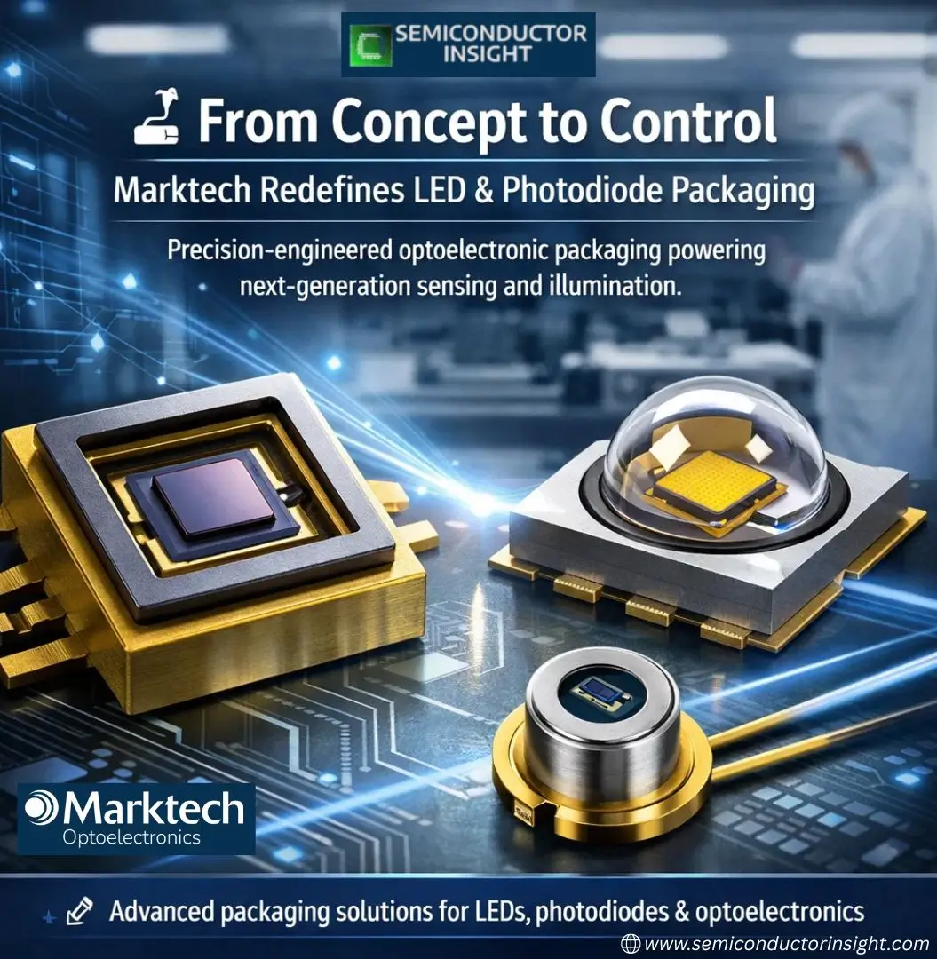
Marktech Optoelectronics Inc., in collaboration with its device manufacturing partner Optrans Corp., has announced the development of new transfer-molded packaging capabilities for LEDs and photodiodes, with first customer availability expected in Q2 2026. The initiative represents a significant step forward in photonics device packaging, addressing growing industry demand for higher reliability, improved optical performance, and scalable manufacturing.
The next-generation packages are engineered to support a broad range of emitter and detector technologies, including conventional LEDs, resonant-cavity LEDs (RCLEDs), and quantum well LEDs (QWLEDs). By using transfer molding, the optical and mechanical structure is formed directly over the device die, enabling tighter control over beam shape, improved environmental protection, and consistent part-to-part performance.
Why Transfer Molding Matters in Photonics Packaging
Unlike traditional packaging approaches such as glob-top epoxy, liquid potting, silicone domes, or discrete lens assemblies transfer molding encapsulates the device in a highly controlled molding process. This method enhances both optical and mechanical integrity while improving long-term reliability.
Key advantages include:
- Improved beam control with reduced stray-light interference
- Exceptional uniformity across production batches
- Enhanced wire-bond protection for rugged operation
- Greater resistance to temperature and humidity stress
- Compact form factors suitable for dense system integration
These characteristics make transfer-molded packages especially well-suited for industrial automation, medical instrumentation, aerospace systems, automotive electronics, and precision measurement equipment, where repeatable optical performance and durability are critical.
Supporting Advanced Emitter Architectures
The new packaging platform is designed to meet the needs of emerging point-source technologies, where optical alignment and beam geometry directly affect system performance. According to Optrans CTO Vince Forte, transfer molding provides the level of optical control, reliability, and manufacturing scalability required for advanced photonic designs particularly in applications where precision and consistency are non-negotiable.
Looking Ahead
With development underway and customer availability targeted for 2026, the Marktech–Optrans collaboration positions both companies at the forefront of high-reliability photonics packaging. As demand grows for compact, durable, and optically precise components, transfer-molded solutions are expected to play a larger role in next-generation sensing and illumination systems.
View Our Most Up-to-Date Related Insights Here:
https://semiconductorinsight.com/report/monitoring-photodiodes-market/
Comments (0)