
Manufacturing Accuracy and Growth across Electrostatic Chuck for Semiconductor Process Market
Electrostatic Chuck for Semiconductor Process Market plays a crucial role in enabling advanced wafer fabrication by ensuring stable wafer positioning during critical manufacturing steps. In semiconductor production, even microscopic variations can affect device performance, making wafer holding systems an essential part of fabrication equipment. Electrostatic chucks (ESCs) rely on electrostatic forces to secure wafers without mechanical pressure, allowing manufacturers to maintain high levels of process consistency across multiple processing stages.
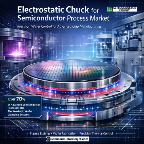
Today, more than 70% of advanced semiconductor fabrication processes rely on electrostatic wafer clamping systems to maintain precision in plasma etching, chemical vapor deposition, and ion implantation processes. With semiconductor nodes shrinking and wafer diameters expanding, ESC systems have become essential for maintaining wafer alignment and uniformity during high-temperature and high-vacuum operations.
Engineering Design behind Electrostatic Wafer Clamping
- Electrostatic chucks operate through Coulombic or Johnsen-Rahbek mechanisms that generate electrostatic attraction between the wafer and the chuck surface. These designs enable strong wafer holding capability while maintaining minimal contamination risk.
- Modern ESC platforms are typically manufactured using ceramic materials such as aluminum nitride and alumina. These materials account for nearly 65% of electrostatic chuck substrate usage due to their high thermal conductivity and electrical insulation properties. Their ability to maintain temperature stability during plasma exposure makes them highly suitable for advanced wafer processing systems.
- In semiconductor fabrication facilities, wafer sizes typically range between 200 mm and 300 mm, with 300 mm wafers representing more than 80% of high-volume production lines globally.
- Electrostatic chucks designed for these wafers must maintain temperature uniformity across hundreds of processing cycles while ensuring repeatable wafer positioning.
Integration with Plasma Etching and Deposition Systems
Electrostatic chucks are deeply integrated into plasma-based semiconductor equipment. Plasma etching tools, which account for nearly 35% of wafer fabrication steps, depend heavily on ESC platforms to maintain wafer stability during high-energy plasma interactions.
During plasma processes, wafers experience extreme temperature fluctuations and ion bombardment. Electrostatic chucks provide controlled wafer cooling through integrated helium backside gas systems. Approximately 60% of plasma processing equipment utilizes backside helium cooling to maintain thermal stability and improve etching accuracy.
Deposition systems, including atomic layer deposition and physical vapor deposition tools, also rely on ESC platforms to ensure uniform film growth across wafer surfaces. Even small deviations in wafer positioning can lead to uneven thin-film layers across integrated circuits.
Materials Innovation in Electrostatic Chuck Platforms
Material science advancements are shaping the development of modern ESC systems. Ceramic electrostatic chucks dominate the market due to their superior durability and contamination resistance.
Aluminum nitride-based chucks represent nearly 50% of ceramic ESC installations in advanced semiconductor manufacturing lines because of their strong thermal conductivity properties. Alumina materials account for a significant portion of cost-efficient ESC production used in mature fabrication technologies.
Surface coating technologies are also improving chuck longevity. Anti-plasma erosion coatings can increase operational lifespan by over 40% compared with conventional ceramic surfaces. This improvement reduces equipment maintenance cycles and improves wafer throughput efficiency.
Wafer Size Evolution and Manufacturing Compatibility
The semiconductor industry has progressively increased wafer size to improve production efficiency. The shift from 200 mm to 300 mm wafers significantly increased the demand for advanced electrostatic chuck designs capable of handling larger substrates.
More than 85% of global semiconductor fabrication capacity currently operates on 300 mm wafer platforms. ESC systems designed for these wafers must maintain consistent clamping force across a surface area exceeding several hundred square centimetres.
As wafer sizes continue evolving for specialized applications such as power electronics and compound semiconductors, electrostatic chucks manufacturers are developing adaptable designs compatible with multiple substrate materials including silicon carbide and gallium nitride.
Expanding Use across Advanced Semiconductor Nodes
As semiconductor devices move toward smaller nodes and higher transistor densities, wafer handling precision becomes even more critical. Electrostatic chucks provide a stable environment required for manufacturing technologies that involve billions of transistors on a single chip.
High-density logic processors, advanced memory architectures, and power semiconductor devices all require stable wafer positioning throughout complex fabrication cycles. The use of electrostatic chuck systems ensures that wafers remain aligned during processes that involve thousands of repeated plasma and deposition steps.
With semiconductor fabrication facilities operating continuously across hundreds of process chambers, ESC platforms remain a foundational component supporting consistent wafer throughput and production reliability.
For a more thorough report, please contact us using our most recent report:
https://semiconductorinsight.com/report/electrostatic-chuck-for-semiconductor-process-market/
Electrostatic Chuck for Semiconductor Process Market continues to gain importance as semiconductor fabrication technologies become increasingly sophisticated. From plasma etching to thin-film deposition, ESC systems enable stable wafer positioning, thermal control, and process consistency across modern semiconductor manufacturing environments.
With advanced materials, sensor integration, and improved thermal management capabilities, electrostatic chuck technology remains a key enabler for precision wafer processing. As fabrication technologies evolve, the role of Electrostatic Chuck systems will remain central to achieving high-accuracy semiconductor production and maintaining process stability across global manufacturing facilities.

Comments (0)