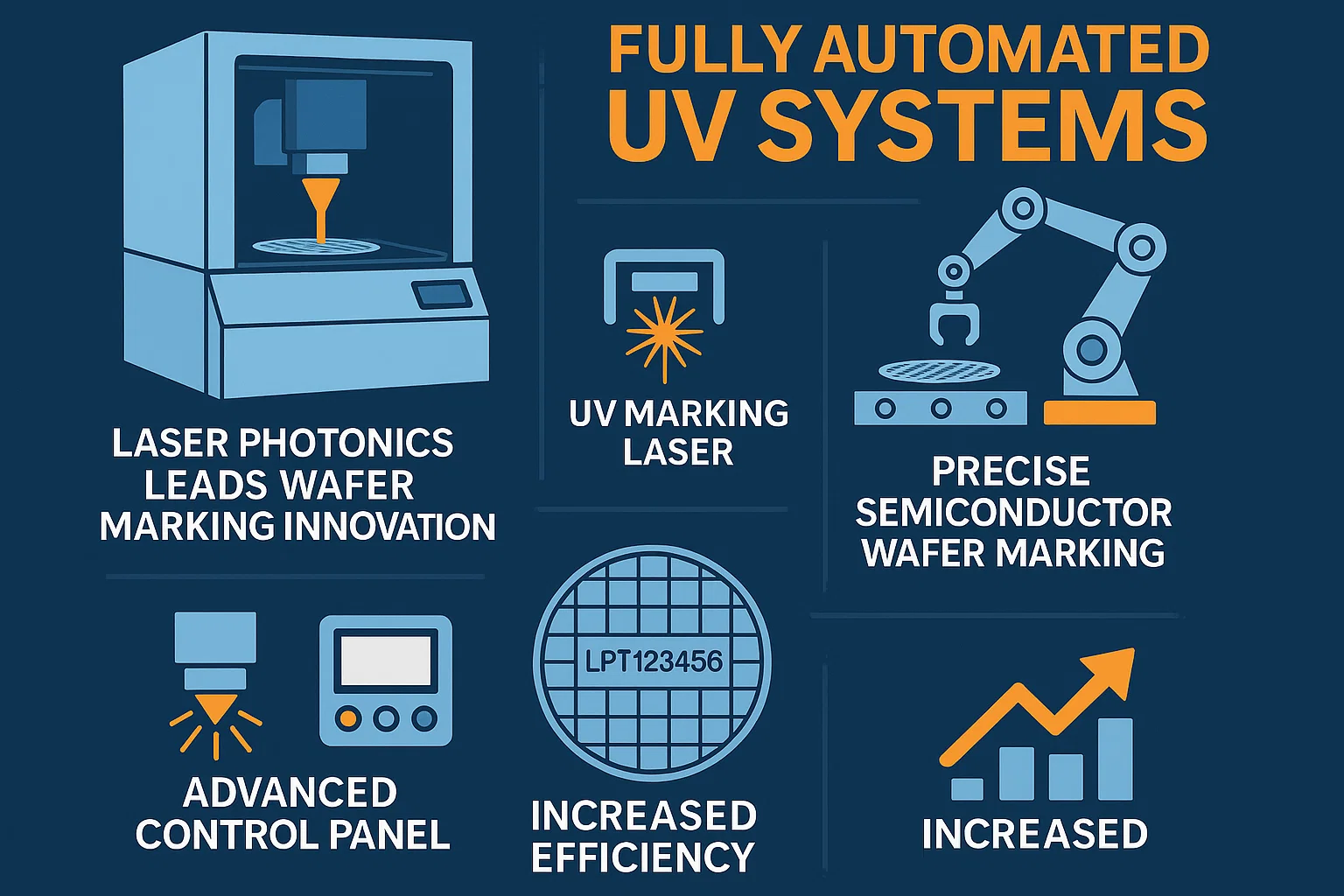
Laser Photonics Leads Wafer Marking Innovation with Fully Automated UV Systems
In the fast-paced world of semiconductors, where nanometers matter and automation is king, the once-niche segment of fully automatic wafer laser marking systems is undergoing a remarkable transformation. As of 2024, the global market for these precision systems is valued at US$ 94.8 million, and it’s projected to reach US$ 158.4 million by 2032, growing at a steady CAGR of 6.7% from 2025 to 2032. What’s fueling this momentum? The answer lies in a convergence of rising semiconductor demand, heightened traceability requirements, fab automation, and technological advancements in laser optics.
Access Your Free Sample Report- Fully Automatic Wafer Laser Marking Systems Market
What Are Fully Automatic Wafer Laser Marking Systems?
Fully automatic wafer laser marking systems are specialized machines that use high-precision lasers—often ultraviolet (UV) or green laser sources—to engrave unique identifiers (such as serial numbers, QR codes, or 2D DataMatrix codes) directly onto silicon or compound wafers. These systems are integral to fab operations, especially for:
· Traceability & Lot Identification
· Process Monitoring & Yield Management
· Quality Control & Regulatory Compliance
· Automation & Data Integration with MES (Manufacturing Execution Systems)
Unlike manual or semi-automatic alternatives, fully automatic systems integrate robotic wafer handling, machine vision alignment, defect detection, and real-time feedback loops—all of which are essential for today’s high-throughput semiconductor fabs.
Market Snapshot (2024–2032): Growth, Drivers, and Challenges
Market Size & Growth Projections
· 2024 Market Value: US$ 94.8 million
· 2032 Forecast: US$ 158.4 million
· CAGR (2025–2032): 6.7%
Key Growth Drivers
1. Semiconductor Boom: Demand for AI chips, 5G, EVs, and IoT devices is pushing fabs to scale production—and with it, wafer marking systems.
2. Automation & Industry 4.0: Fully automatic laser systems enable non-contact marking, MES integration, and reduced human error.
3. Miniaturization Trends: As wafers shrink and complexity increases, high-resolution UV lasers become essential for non-damaging, ultra-fine marking.
4. Traceability Regulations: Both consumer electronics and defense sectors demand traceability from wafer to finished chip.
Challenges
· High CapEx for cutting-edge systems
· Requirement for cleanroom-certified, low-particulate machinery
· Limited awareness in developing semiconductor ecosystems
Latest Developments: A Closer Look at the Industry in 2024–2025
The past year has seen a wave of innovation and strategic activity in the wafer laser marking space, particularly from U.S.-based Laser Photonics Corporation (LPC) and its subsidiary CMS Laser.
Laser Photonics Expands Semiconductor Product Line (Dec 2024)
In a strategic announcement in December 2024, Laser Photonics Corp. launched a suite of advanced wafer processing systems tailored specifically for semiconductor fabs. These systems offer laser wafer dicing, scribing, and marking—blending three critical processes into one fully automated machine.
Highlights:
· Ultraviolet (UV) laser sources for ultra-fine marking without microstructure damage.
· Integration with robotic wafer handlers, machine vision, and AI-based inspection.
· Modular designs capable of handling multiple wafer sizes (200mm, 300mm).
· Support for encrypted QR/Data Matrix codes and direct MES linking.
The move is a response to increased customer demand for fab‑level automation and inline quality assurance. LPC’s systems reportedly reduce wafer damage rates by over 40% compared to traditional thermal or chemical marking techniques.
Download Sample Report PDF- Fully Automatic Wafer Laser Marking Systems Market
Laser Photonics and CMS Laser Double Down on R&D (Feb 2025)
In early 2025, Laser Photonics unveiled a robust R&D expansion with Control Micro Systems (CMS Laser). The focus: developing laser systems capable of marking next-gen semiconductor materials like GaN, SiC, and compound wafers, which are increasingly used in high-power and RF applications.
Innovations Underway:
· Customizable laser heads for precise depth control and minimal heat-affected zones.
· Wafer flipping and dual-side marking capabilities.
· Integration with AI-powered defect detection before and after marking.
· New stacker-compatible designs to enable smooth fab-to-tool automation.
These efforts are crucial as fabs shift toward heterogeneous integration and advanced packaging—processes that demand fine, durable wafer markings for traceability throughout multi-chip modules.
Broader Market Trends and Emerging Technologies
Beyond the activities of LPC, the market is shaped by a broader technological landscape. Companies like IPG Photonics, Coherent, and Trumpf are introducing picosecond and femtosecond UV/green lasers, enhancing marking precision below 10 μm line width.
AI and Machine Vision
Modern systems include real-time OCR, barcode validation, and AI-driven defect classification—minimizing rework and boosting throughput.
Modular System Designs
To meet fab needs, systems are now modular—allowing OEMs and IDMs to scale capacity or swap laser heads without full system overhauls.
Cybersecurity in Traceability
Encrypted QR codes and secure cloud syncing ensure wafer traceability data is protected against IP theft and tampering.
Key End-Use Applications and Buyer Segments
Primary Users
· Semiconductor Foundries (e.g., TSMC, GlobalFoundries)
· IDMs (e.g., Intel, Samsung, Infineon)
· OSATs (Outsourced Semiconductor Assembly and Test providers)
· Research Labs and Pilot Fabs
Applications
· Wafer ID marking
· Pre-dicing scribing
· Lot & batch tracking
· In-line quality assurance
· Advanced packaging traceability
As advanced nodes (<5nm) and 3D stacking grow more prevalent, these systems will become even more indispensable.
Competitive Landscape: Who’s Leading the Charge?
|
Company |
Focus |
Key Products |
Competitive Edge |
|
Laser Photonics |
UV laser marking & dicing |
LPC WaferMark Series |
Fully integrated, U.S. based, fab-ready |
|
CMS Laser |
Custom laser automation |
OEM laser subsystems |
High-end R&D, robotic integration |
|
Coherent Corp. |
Industrial laser tech |
AVIA UV Laser Series |
High throughput, precision marking |
|
IPG Photonics |
Fiber & green lasers |
Marking solutions for compound semis |
Femtosecond tech, minimal thermal impact |
|
Trumpf |
Precision marking & welding |
TruMark Series |
Trusted across high-tech fabs |
Future Outlook: What’s Next for Wafer Laser Marking Systems?
1. Growth in Compound Semiconductors
As SiC and GaN become mainstream in power electronics, laser systems must adapt to new material reflectivity and absorption characteristics.
2. Rise of Smart Fabs
Expect more fully automatic systems with edge computing, real-time analytics, and machine learning to predict tool wear and optimize marking parameters.
3. Green Laser and Femtosecond Adoption
To meet the demands of advanced-node chips, femtosecond and green laser systems will see wider adoption due to their non-thermal, ultra-fine engraving capabilities.
4. Global Localization
With chip sovereignty rising globally (e.g., U.S. CHIPS Act, EU Chips Act, India’s DLI scheme), localized manufacturing will spur regional demand for marking systems.
Click Here To Download Full Sample Report- Fully Automatic Wafer Laser Marking Systems Market
Precision, Performance, and the Power of Data
The fully automatic wafer laser marking systems market is no longer a back-end afterthought—it’s a strategic lever for traceability, automation, and quality assurance in fabs worldwide. With a projected value of US$ 158.4 million by 2032, this market segment is scaling in sync with semiconductor complexity.
Companies like Laser Photonics and CMS Laser are setting benchmarks in customization, integration, and R&D—transforming wafer marking from a process step to a high-value differentiator. As fabs race toward autonomy, green manufacturing, and defect-free chips, laser marking systems will not just follow—they’ll lead.
Comments (0)