
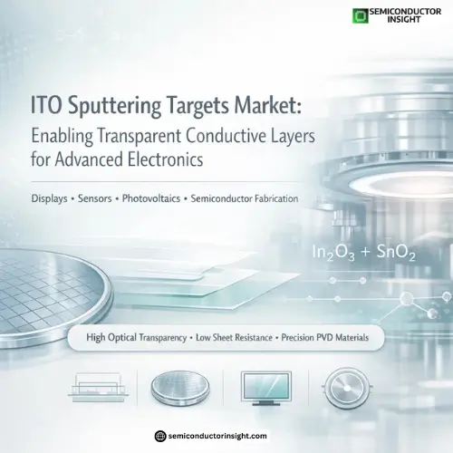
Indium Tin Oxide Target Insights Supports Scalable Manufacturing in Advanced Electronics
Indium Tin Oxide (ITO) is a transparent conductive oxide essential to modern electronics. Its combination of high optical transparency (>85%) and excellent electrical conductivity makes it the material of choice in flat panel displays (FPDs), touch screens, thin-film photovoltaics, organic light-emitting diodes (OLEDs), and various MEMS and sensor applications. The sputtering target a dense, high-purity ITO material is the source from which thin films are deposited onto substrates through physical vapor deposition (PVD) processes.
In the context of semiconductors, ITO is not just a film; it’s a functional layer that enables critical device characteristics such as responsive touch interfaces, low-loss transparent electrodes, and efficient charge collection. As displays, wearable, and smart sensors proliferate, demand for high-quality ITO sputtering targets has grown in lockstep.
Expanded Applications beyond Displays
While flat panel displays (LCD, OLED) historically dominated ITO demand, new applications are broadening market uptake:
- Mini-LED and Micro-LED Displays: Higher brightness and contrast demands drive thicker, high-uniformity ITO layers to support efficient current spreading.
- Flexible Electronics: ITO targets tailored for flexible substrates (e.g., polyimide) require unique stress and adhesion profiles.
- Photonic Sensors and MEMS: Transparent electrodes in advanced sensors, ranging from LiDAR to biometric modules, rely on localized ITO deposition.
- Photovoltaics and Smart Windows: ITO target use in thin-film PV and electrochromic devices further extends material demand into energy and building tech sectors.
These expansions diversify the market beyond traditional consumer displays into growth segments where optical performance and electrical reliability are equally critical.
Global Market Shifts and Recent Innovation
- Supply Chain Tightening: Indium a rare element is a constrained resource. Fluctuations in indium pricing and supply, influenced by upstream mining outputs and commodity cycles, have impacted target availability. Several regions have reported 15-20% cost variation year-to-year in raw indium feedstock prices, prompting target manufacturers to innovate in material utilization and recycling.
- Facility Upgrades in Asia: East Asian semiconductor hubs particularly South Korea, Taiwan, and China continue to invest in display fabs and advanced packaging infrastructure. Rapid build-out of OLED and Mini-LED facilities is creating corresponding demand for high-throughput ITO target production.
- Hybrid and Nano-Structured Targets: Recent R&D focuses on composite targets that integrate optimized grain structures and engineered dopant gradients to improve film uniformity and lower target erosion rates. These innovations support higher deposition speeds without compromising optical clarity.
- Recycling and Circular Economy Strategies: With increasing material scarcity, some manufacturers are adopting ITO target recycling programs that reclaim indium and tin from spent targets. This chemical recovery not only reduces waste but also partially mitigates raw material cost exposure.
Production Chemistry and Quality Constraints
Producing ITO sputtering targets is a chemical engineering challenge requiring precise control over raw material stoichiometry, oxygen content, and densification processes. Ceramic Powder preparation involves careful blending of indium oxide and tin oxide precursors under controlled atmospheres to ensure homogeneous distribution. Subsequent pressing and sintering at high temperatures (>1,500 °C in some processes) must maintain uniform chemical composition and avoid segregation or volatile loss.
Process control also extends to target machining and finishing surface roughness, flatness, and microstructure must meet tight tolerances to avoid arcing and uneven sputter yields in high-power PVD chambers used in semiconductor fabs.
These manufacturing steps are inherently chemical in nature, influencing defect density, target lifetime, and sputter rate uniformity. High-performance targets translate directly into higher uptime and less film variance on semiconductor and display wafers.
Please Take a Look at Our Updated Report before Continuing:
https://semiconductorinsight.com/report/indium-tin-oxide-ito-sputtering-targets-market/
Increasing Demand from High-Resolution and Premium Displays
With consumer electronics evolving toward ultra-HD, curved, and foldable formats, the material demands on ITO films are rising. Higher resolution demands larger sputtering targets and more frequent target replacement due to increased throughput. In many leading fabs, target change intervals now follow strict preventive maintenance schedules tied to total deposited area and defect rate thresholds.
Many manufacturers now track usage in terms of square meters of film deposited per target rather than simply hours of use reflecting production realities in high-volume display lines and advanced sensor arrays.
Environmental and Regulatory Context
ITO target production and disposal intersect with environmental regulations governing heavy metal usage, particulate emissions, and energy consumption. Target manufacturers are therefore investing in clean processing technologies, improved waste handling, and energy-efficient kiln and furnace systems to meet global standards and reduce carbon footprint.
Recycling programs and closed-loop indium recovery initiatives are also aligned with broader sustainability commitments in the semiconductor supply chain.
The outlook for the ITO sputtering targets market remains tied to the broad trajectory of advanced electronics and semiconductor adoption. Continued expansion of:
- OLED and Mini-LED display fabs
- EV and industrial sensor networks
- Transparent electrodes in next-gen photovoltaics
- Smart device interfaces with embedded touch and gesture recognition
This will underpin demand for high-performance, reliable ITO target materials. Technical challenges such as target lifetime optimization, novel material composites, and recycling advancements are likely to shape supplier differentiation in the coming years.
For semiconductor and display OEMs, aligning with target suppliers that offer consistent chemical quality, scalable production capacity, and robust global support networks will be fundamental to sustaining yield and performance at next-generation technology nodes.

Comments (0)