
Imec and EV Group Advance Wafer-to-Wafer Hybrid Bonding for Next-Generation Semiconductor Architectures
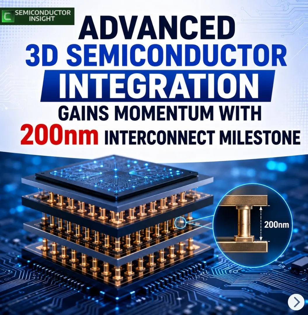
At the 2026 IEEE Electronic Components and Technology Conference (ECTC), imec and EV Group announced a major breakthrough in wafer-to-wafer hybrid bonding technology, demonstrating a highly reliable process at an ultra-fine 200nm copper interconnect pitch. The achievement marks a significant advancement in the evolution of advanced semiconductor packaging and 3D integration technologies that are expected to power future AI-driven computing systems.
The milestone reflects the semiconductor industry’s growing transition toward vertically stacked chip architectures as traditional transistor scaling approaches become increasingly complex and costly. Advanced hybrid bonding technologies are now viewed as critical enablers for achieving higher interconnect density, improved performance efficiency, and faster data transfer in next-generation semiconductor devices.
The latest demonstration by imec and EVG was achieved using a test vehicle containing four layers of routable interconnects pre-processed on each wafer before bonding. One of the most notable accomplishments was the achievement of a post-bond copper pad alignment accuracy below 40 nanometres across an entire 300mm wafer, representing a world-first level of overlay precision for this class of technology.
- Such ultra-precise alignment is essential for enabling future logic-to-logic and memory-to-logic stacking applications, where billions of microscopic interconnections must function with extremely high electrical reliability and minimal signal loss.
- These capabilities are becoming increasingly important as industries demand more powerful and energy-efficient computing platforms for artificial intelligence, high-performance computing (HPC), data centres, autonomous systems, and advanced edge computing applications.
- The breakthrough is closely aligned with imec’s broader CMOS 2.0 scaling paradigm, which envisions a shift from conventional monolithic chip designs toward modular, vertically integrated architectures.
- Under this approach, system-on-chip (SoC) designs are divided into specialized functional layers that are interconnected using advanced 3D packaging and wafer bonding technologies.
According to Zsolt Tokei, the achievement was made possible through the co-optimization of multiple critical process technologies, including the use of silicon carbon nitride (SiCN) dielectric materials, advanced chemical mechanical polishing (CMP), and highly controlled copper pad engineering. The process flow was specifically optimized to ensure exceptional surface flatness and nanometer-scale recess control required for successful fine-pitch hybrid bonding.
A major contributor to the milestone was EVG’s advanced wafer bonding platform, the GEMINI FB system, which enabled the unprecedented overlay precision necessary for maintaining high electrical yield at extremely small interconnect dimensions.
As semiconductor architectures continue evolving toward greater complexity, hybrid bonding is expected to become one of the foundational technologies supporting future chiplet integration and heterogeneous computing systems. The ability to stack logic and memory layers with ultra-high density interconnects allows semiconductor manufacturers to overcome physical limitations associated with traditional planar scaling while improving bandwidth, latency, and power efficiency.
Paul Lindner emphasized that the long-standing collaboration between EVG and imec demonstrates the importance of close cooperation between research institutions and semiconductor equipment providers in driving meaningful advances in process technology. Over the past several decades, partnerships of this kind have played a critical role in accelerating innovation across the global semiconductor ecosystem.
The companies also indicated that their roadmap extends beyond the current 200nm interconnect pitch milestone. Future development efforts will focus on achieving even finer pitch hybrid bonding capabilities to support increasingly demanding AI and advanced computing applications that require unprecedented interconnect density and integration performance.
The announcement comes at a time when semiconductor manufacturers worldwide are investing heavily in advanced packaging technologies as a strategic pathway for sustaining performance growth in the post-Moore’s Law era. Technologies such as hybrid bonding, chiplet architectures, and 3D stacking are rapidly becoming central to the future of semiconductor design and manufacturing.
A Review of Our Comprehensive Analysis-Related Report: https://semiconductorinsight.com/report/wafer-to-wafer-w2w-hybrid-bonding-market/

Comments (0)