
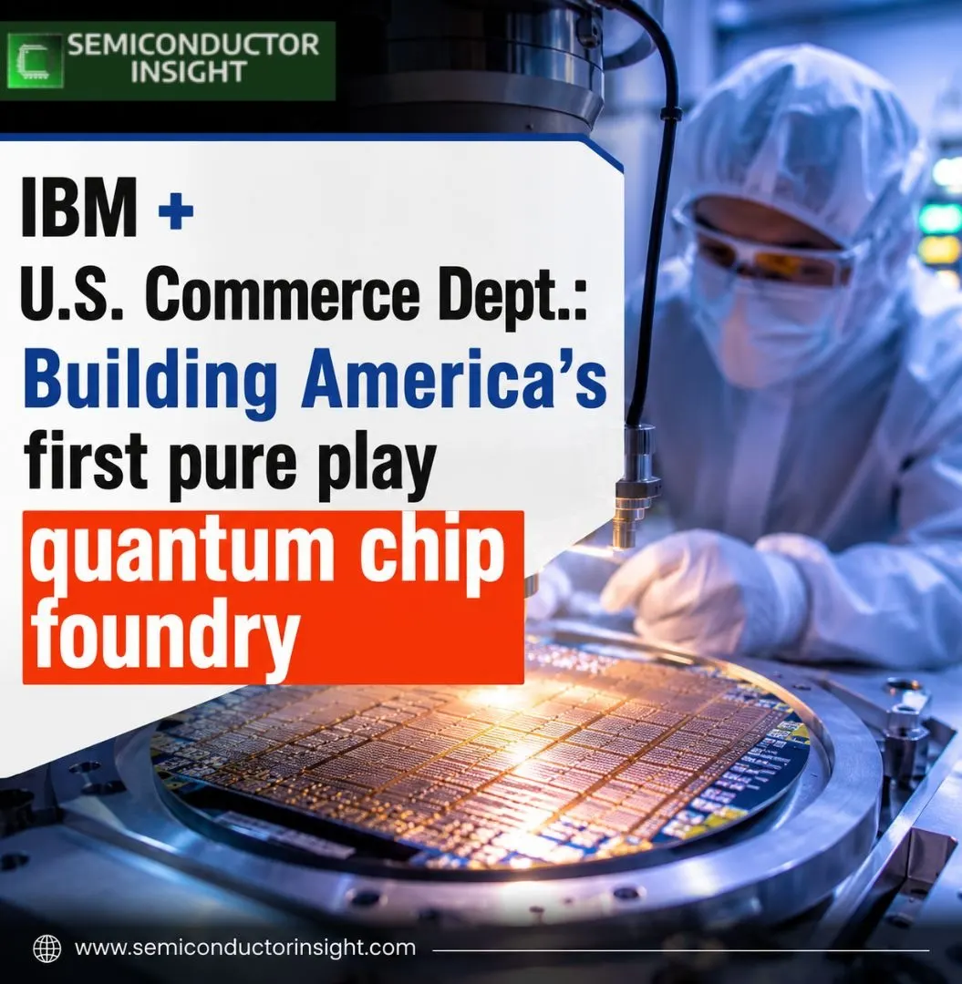
IBM and U.S. Department of Commerce launch Anderon America’s first pure‑play quantum wafer foundry
In a landmark move to anchor the United States at the center of the emerging quantum economy, IBM and the U.S. Department of Commerce have signed a Letter of Intent (LOI) to establish Anderon, the nation’s first standalone, pure‑play quantum chip foundry. Backed by a $1 billion CHIPS R&D incentive from the Department of Commerce and an equal cash commitment from IBM plus significant IP, manufacturing assets, and expert personnel Anderon will be headquartered in Albany, New York and operate a state‑of‑the‑art 300‑millimeter quantum wafer fabrication facility.
Quantum research has produced striking breakthroughs in algorithms, materials and qubit design. Anderon represents the next critical phase: converting those breakthroughs into volume‑manufacturable wafers that can power practical quantum systems. By focusing exclusively on quantum wafer fabrication, Anderon aims to supply multiple hardware vendors and accelerate the commercialization of scalable quantum technologies.
This initiative is one of the most significant commitments by the U.S. Government to date in quantum R&D, said Department of Commerce leadership. The project targets domestic supply‑chain resilience, high‑skilled job creation, and enhanced national security while supporting a quantum industry that could generate up to $850 billion in economic value by 2040.
Why Anderon matters?
- National scale and resilience: Anderon aims to produce the majority of the world’s quantum wafers from a secure, U.S.‑based foundry, reducing dependence on fragmented global supply chains.
- Pure‑play foundry model: Operating independently as a wafer‑only company enables Anderon to serve multiple quantum hardware vendors, fostering an open ecosystem where innovation and competition can thrive.
- Economic and workforce impact: The combined public‑private investment will create high‑paying manufacturing and R&D jobs and catalyze regional and national industry growth.
- Security and sovereignty: A domestic source of quantum wafers strengthens technological resilience for defense, critical infrastructure, and sensitive industries.
Anderon will launch with advanced 300 mm wafer processes tailored for superconducting qubit architectures and supporting electronics, with plans to expand into additional quantum modalities over time. Its planned capabilities include superconducting wiring, through‑silicon vias (TSVs), bumping, dedicated process design kits (PDKs), in‑line wafer testing and characterization, and production routes designed for rapid iteration and industrial reliability.
These manufacturing milestones are built on IBM’s decades of investment in quantum computing and wafer fabrication. IBM will contribute $1 billion in cash to Anderon, plus valuable intellectual property, tools and a specialized workforce. As Anderon scales, additional investors are expected to join, broadening the capital and technical base of the venture.
Voices from the partnership
IBM has pioneered quantum computing for decades, said Arvind Krishna, Chairman and CEO of IBM. Our work in silicon wafer fabrication has been a key to IBM’s success and will be critical to enable a broader quantum technology landscape that will reshape global innovation and economic competitiveness. With the support of the U.S. Department of Commerce, Anderon will be well‑positioned to fuel America’s fast‑growing quantum technology industry.
Commerce leadership framed the CHIPS investment as a decisive push to accelerate American innovation. These strategic quantum technology investments will build on our domestic industry, creating thousands of high‑paying American jobs while advancing American quantum capabilities, said Secretary of Commerce Howard Lutnick. Bill Frauenhofer, Executive Director of Semiconductor Investment and Innovation, added that the incentives will bolster technological resilience across defense, advanced materials, biopharma discovery, financial modeling and energy systems.
From day one, Anderon is designed to be more than a factory it aims to serve as the anchor of a national ecosystem for quantum wafer manufacturing. That ecosystem will include fabless quantum hardware startups, tool and materials suppliers, test and packaging providers, academic collaborators and downstream integrators. By offering production‑grade wafers and the process toolkits needed to iterate and scale, Anderon seeks to lower barriers to entry for innovators and shorten the path from prototype to product.
- For quantum hardware developers, Anderon offers predictable access to high‑quality wafers, enabling faster experimentation and larger‑scale deployments.
- For cloud providers and system integrators, it promises more reliable supply chains and the ability to plan capacity growth with greater confidence.
- For policy makers and national security stakeholders, Anderon represents a concrete capability that aligns industrial policy with strategic technology objectives.
Although Anderon will be U.S.‑based and focused on domestic manufacturing resilience, its pure‑play model is explicitly designed to serve global quantum vendors. By making industrial‑grade wafers available to a broad set of developers, Anderon could accelerate cross‑border collaboration and standardization in quantum device fabrication while keeping critical supply and know‑how anchored in the United States.
The IBM-DoC LOI to create Anderon marks a pivotal shift: public funding and corporate leadership are converging to move quantum technology from laboratory novelty toward industrialized manufacture. If realized at scale, Anderon could reshape the quantum hardware landscape, spur economic growth, strengthen national security, and help the U.S. capture outsized value from the coming quantum era.
Take a Quick Glance at Our In-Depth Analysis Relevant Report: https://semiconductorinsight.com/report/superconducting-quantum-chip-market/

Comments (0)