
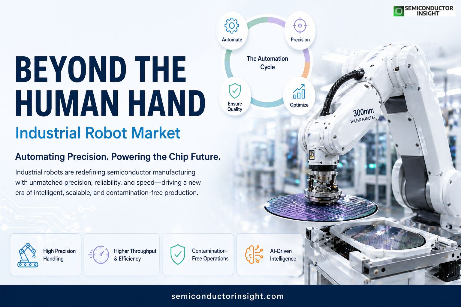
How the Industrial Robot Market is Transforming Global Chip Manufacturing beyond the Human Hand?
The modern semiconductor fabrication facility operates under a physics regime that humans are physically incapable of navigating. While much of the industry discourse focuses on nanometer shrinks and High-NA EUV light sources, the unsung hero of the past five years has been the mechanical arm.
While observing capital expenditure trends, it is impossible to ignore that the global operational stock of industrial robots has climbed to approximately 4.7 million units as of 2025, reflecting a steady 9% year-over-year increase in automation density.
For the semiconductor sector specifically, this is not just about labor replacement; it is about the operational necessity of moving silicon wafers with zero particle contamination and sub-micron precision.
- In 2024, global industries installed 542,000 new industrial robots, marking the second-highest installation volume recorded.
However, what is statistically significant for semiconductor analysts is the shift in demand drivers. Historically, the automotive sector dictated robot sales; but currently, the electronics and semiconductor sub-segments are outpacing traditional automotive demand.
Discover the updated report details through the full overview: https://semiconductorinsight.com/report/industrial-robot-market/
Smart Robotics Design Types Transforming Industrial Performance
To analyse capital investments properly, one must distinguish between the specific kinematics deployed on the cleanroom floor. Not all robots are created equal, and their prevalence signals different manufacturing strategies.
- SCARA (Selective Compliance Assembly Robot Arm):These are the workhorses of assembly and test. In the backend facilities, SCARA robots dominate due to their rigid vertical stiffness combined with high-speed horizontal agility.
For instance, when sorting chips after dicing or placing components onto substrates, the SCARA design offers a cycle time advantage that Cartesian systems cannot match.
- Articulated Robots (6-Axis):While traditionally associated with automotive welding, compact 6-axis arms are increasingly appearing in semiconductor metrology and handling of FOUPs (Front Opening Unified Pods). Their dexterity allows for complex angular movements that fixed-path systems struggle with.
- Cartesian (Gantry) Systems:These remain the standard for older 200mm fabs. They are prized for their modularity and are often custom-built for specific linear motion tasks, such as moving heavy reticles or handling large substrates in panel-level packaging.
- Collaborative Robots (Cobots):The data suggests a massive shift toward human-robot interaction. In North America alone, collaborative robot orders totaled 7,212 units in 2025, representing 19.6% of all robot orders. In the semiconductor world, cobots are gaining traction in labs and maintenance bays, working alongside technicians to handle delicate calibration tasks without safety cages.
The 300mm Tipping Point and the Rise of the Dual Arm
The industry is currently witnessing a structural shift driven by wafer size. Approximately 63% of the current semiconductor robot market is now dedicated to 300mm wafer handling systems. This is critical because 300mm wafers are significantly heavier and more fragile than their predecessors, necessitating advanced vibration control and end-effector design.
Furthermore, leading-edge foundries are moving toward dual-arm modular architectures. About 18% of new system launches now feature dual-arm configurations, allowing for wafer swapping where one arm retrieves a raw wafer while the other places a processed one back into the cassette. This reduces idle time and increases throughput per square foot of cleanroom space. We are seeing a specific surge in demand for vacuum robots capable of handling EUV (Extreme Ultraviolet) mask blanks, where the margin for error is effectively zero nanometers.
Geographic Distribution of Installations
Asia-Pacific continues to act as the gravity well for industrial robotics, absorbing the majority of global supply. Specifically, China alone accounted for 54% of the global robot supply in 2025. However, from a semiconductor perspective, the story is more nuanced. While China leads in volume for legacy chips, Taiwan and South Korea lead in density for advanced nodes. This is reflected in the installed base of high-precision vacuum robots, which are heavily concentrated in Hsinchu and Gyeonggi-do.
Trending Brands Dominating the Semiconductor Floor
While large conglomerates like Fanuc and ABB dominate the general industrial landscape, the semiconductor-specific market has specialized leaders. Based on industry equipment interfaces and supply chain checks, the trending brands influencing wafer handling include:
- Yaskawa Electric (Motoman):Heavily cited for their reliability in dry pumps and vacuum environments, they maintain a stronghold in etch and deposition tool integration.
- Denso Wave:Historically significant for their high-speed SCARA units, Denso remains a top choice for pick-and-place in high-mix, low-volume test floors.
- Kawasaki Robotics:Known for heavy-payload handling, they are increasingly visible in the backend packaging lines where substrates are larger and heavier.
- EPSON Robots:Documented as a major player in the SCARA and 6-axis space for general assembly automation used in chip packaging.
- Universal Robots (Teradyne):While not a cleanroom robot strictly, UR cobots are trending in semiconductor equipment maintenance and calibration labs, as highlighted by the 28.6% Q4 share of cobot orders in industrial automation.
From a hardware component perspective, the demand is spilling over into vision systems and actuators. With 42% of global capital investments in this sector now reportedly flowing toward AI-based robot optimization, the physical robot arm is becoming a data node. We are moving toward a state where the robot not only moves the wafer but also scans it in transit, identifying macro-defects before the wafer even reaches the inspection tool.
Boosting Workflow Productivity
As a final analytical note, watch the velocity metrics. In 2025, the semiconductor industry officially moved past the talent shortage phase into the automation necessity phase.
With approximately 65% of 300mm fabs now utilizing fully automated material handling systems (AMHS), the next efficiency frontier is not lithography speed but the dead time between process steps.

Comments (0)