How Does Wafer Bonding Equipment Impact Semiconductor Manufacturing?
Wafer Bonding Equipment Overview
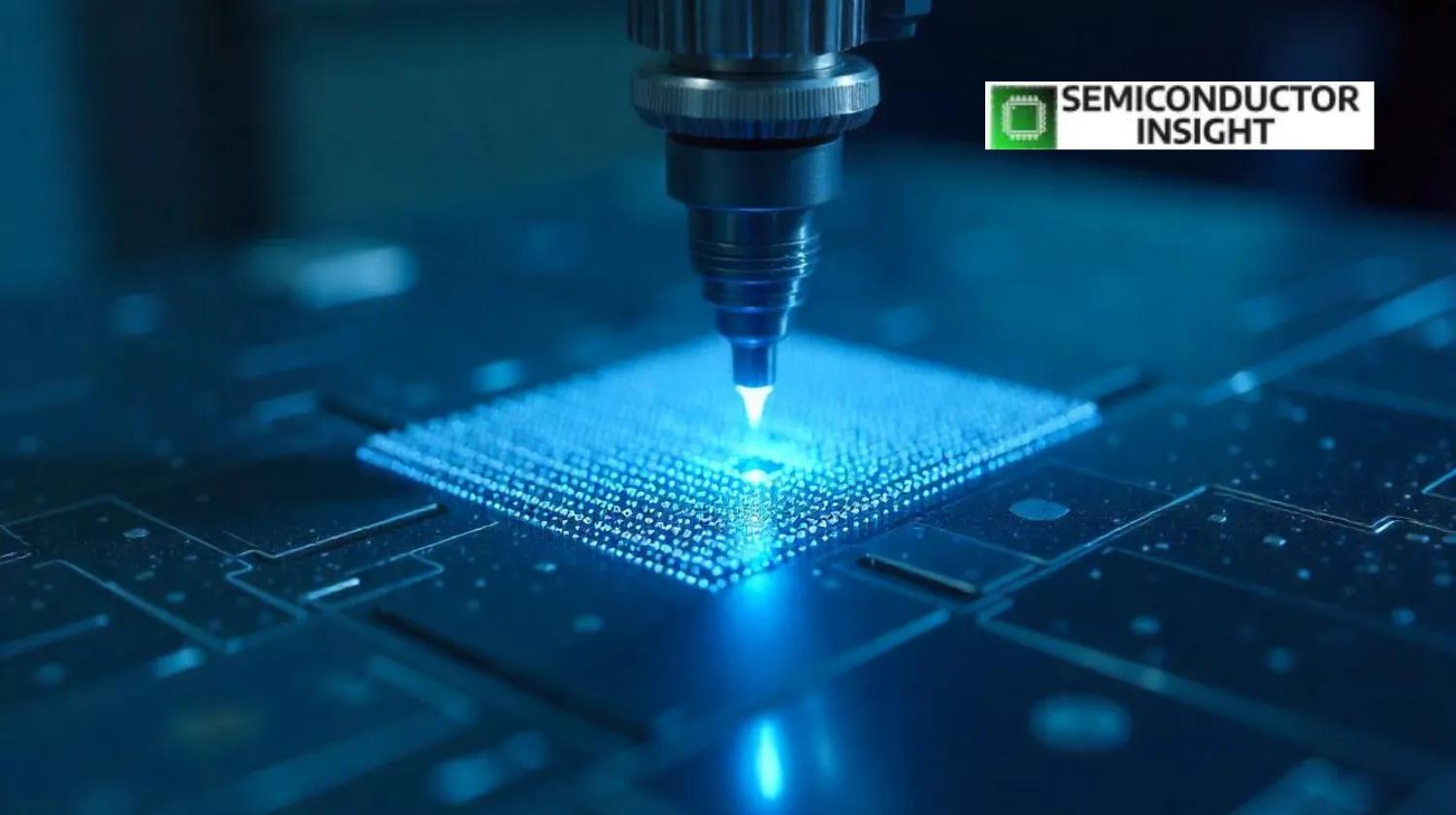
Wafer bonding technology plays a critical role in semiconductor manufacturing, enabling the integration of diverse materials and enhancing device performance. Semiconductor wafer bonding processes are essential for fabricating advanced devices, including MEMS, sensors, and 3D integrated circuits.
Global Wafer Bonding Equipment Market Size and Forecast
Market Size, Share, and Growth
The global wafer bonding equipment market was valued at USD 1.2 billion in 2023 and is projected to reach USD 2.3 billion by 2032, growing at a CAGR of 7.1%. This growth is driven by the increasing demand for MEMS devices, sensors, and advanced packaging solutions.
How Does Wafer Bonding Equipment Impact Semiconductor Manufacturing?
Wafer bonding equipment significantly impacts semiconductor manufacturing in several ways:
- Material Integration: Enables bonding of dissimilar materials for complex device structures.
- Enhanced Performance: Improves electrical and thermal properties of semiconductor devices.
- Miniaturization: Facilitates the creation of compact and high-performance devices.
- Increased Yield: Enhances manufacturing efficiency and reduces defect rates.
- Cost Efficiency: Optimizes production processes, lowering overall manufacturing costs.
Growth Trends in Semiconductor Wafer Bonding Technology
Several key trends are shaping the wafer bonding technology landscape:
- Adoption of 3D Integration: Increasing use of wafer bonding for 3D integrated circuits.
- Advanced Packaging: Growth in wafer-level packaging solutions.
- MEMS Expansion: Rising demand for MEMS wafer bonding in consumer and industrial applications.
- Hybrid Bonding: Development of hybrid bonding techniques for improved performance.
- Automation Integration: Enhanced automation for higher precision and throughput.
Demand for Wafer Bonding in MEMS and Sensors
Wafer bonding is crucial for the production of MEMS devices and sensors:
- MEMS Fabrication: Enables precise assembly of micro-scale components.
- Sensor Integration: Facilitates multi-functional sensor development.
- Biomedical Devices: Supports the creation of microfluidic and biosensor devices.
- Optoelectronic Applications: Assists in manufacturing photonic and optical devices.
- Automotive Sensors: Critical for safety and performance sensors in vehicles.
Wafer Bonding Equipment Key Players in the Market
Leading companies in the wafer bonding equipment market include:
- EV Group (EVG): Known for innovative wafer bonding and lithography equipment.
- SÜSS MicroTec: Specializes in advanced wafer bonding solutions.
- Tokyo Electron Limited: Offers a range of semiconductor manufacturing equipment.
- Kulicke & Soffa Industries, Inc.: Provides wafer bonding and assembly solutions.
- ASM International: Focuses on advanced semiconductor packaging technologies.
Wafer Bonding Equipment Future Growth Opportunities
The wafer bonding equipment market presents several promising growth opportunities:
- MEMS and IoT Devices: Rising demand for miniaturized and high-performance devices.
- Photonics Integration: Growth in photonic device manufacturing.
- Advanced Packaging: Expansion of wafer-level and hybrid packaging solutions.
- Biomedical Applications: Increased use in medical sensors and diagnostic devices.
- Regional Market Expansion: Growing investments in Asia-Pacific and North America.
Conclusion
Wafer bonding equipment is essential for advancing semiconductor manufacturing, enabling the integration of complex device structures and enhancing performance. As demand for MEMS, sensors, and advanced packaging continues to rise, the wafer bonding equipment market is poised for significant growth.
FAQs
Q: What are the key driving factors and opportunities in the wafer bonding equipment market?
A: Key drivers include the growing demand for MEMS devices, advanced packaging solutions, and increased adoption of 3D integration. Opportunities exist in photonics, biomedical applications, and IoT devices.
Q: Which region is projected to have the largest market share?
A: Asia-Pacific dominates the market due to its strong semiconductor manufacturing base and significant investments in advanced technologies.
Q: Who are the top players in the global wafer bonding equipment market?
A: Leading companies include EV Group, SÜSS MicroTec, Tokyo Electron Limited, Kulicke & Soffa Industries, Inc., and ASM International.
Q: What are the latest technological advancements in the industry?
A: Innovations include hybrid bonding techniques, automation integration, and advanced wafer-level packaging solutions.
Shubham K
Shubham is a seasoned market researcher specializing in the semiconductor industry, providing in-depth analysis on emerging trends, technological advancements, and market dynamics. With extensive experience in semiconductor manufacturing, supply chain analysis, and competitive intelligence, Shubham delivers actionable insights that help businesses navigate the evolving landscape of chip design, fabrication, and applications. His expertise spans key areas such as AI-driven semiconductors, advanced packaging, memory technologies, and foundry trends. At SemiconductorInsight, Shubham combines data-driven research with strategic foresight, offering thought leadership that empowers industry professionals, investors, and technology innovators to make informed decisions.
Comments (0)