How Do SiC Wafer Defect Inspection Systems Enhance Semiconductor Quality?
SiC Wafer Defect Inspection Systems Overview
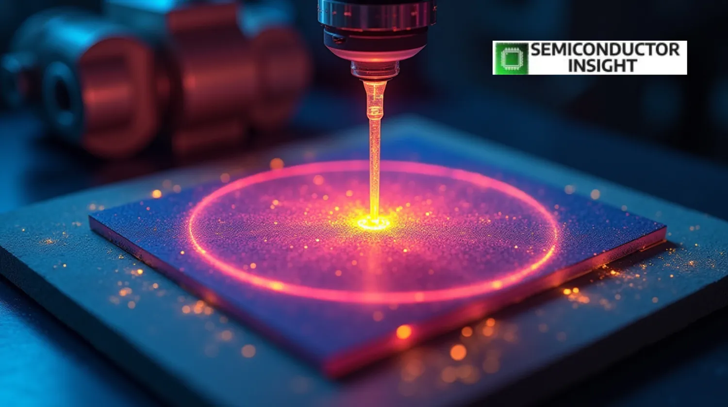
Silicon carbide (SiC) wafer defect inspection systems play a critical role in enhancing semiconductor quality. As SiC gains prominence in power electronics, ensuring defect-free wafers becomes crucial. SiC wafer defect detection systems utilize advanced technologies to identify imperfections, enabling manufacturers to produce high-performance semiconductors.
Global SiC Wafer Defect Inspection System Market Size and Forecast
Market Size, Share, and Growth
The global SiC wafer defect inspection system market was valued at USD 300 million in 2023 and is projected to reach USD 850 million by 2032, growing at a CAGR of 12.5%. This growth is driven by the increasing demand for high-quality SiC wafers in power electronics and the critical importance of defect inspection in SiC wafer manufacturing.
How Do SiC Wafer Defect Inspection Systems Enhance Semiconductor Quality?
SiC wafer defect inspection systems enhance semiconductor quality through the following ways:
- Accurate Defect Detection: Advanced inspection tools precisely identify surface and subsurface defects.
- Improved Yield: Detecting and eliminating defective wafers increases manufacturing yield.
- Enhanced Performance: Defect-free SiC wafers contribute to better electrical performance in semiconductors.
- Cost Reduction: Early defect detection minimizes waste and lowers production costs.
- Reliability Assurance: Ensures long-term reliability and durability of power electronic devices.
Importance of Defect Inspection in SiC Wafer Manufacturing
Defect inspection is crucial in SiC wafer manufacturing for several reasons:
- Quality Control: Ensures wafers meet stringent industry standards.
- Device Performance: Directly impacts the efficiency and reliability of power devices.
- Cost Efficiency: Reduces losses associated with defective wafers.
- Market Competitiveness: High-quality wafers enhance brand reputation and market share.
- Safety Assurance: Critical for applications in automotive and industrial power electronics.
Optical vs. Non-Optical SiC Wafer Defect Inspection Techniques
SiC wafer defect inspection utilizes both optical and non-optical methods:
- Optical Inspection: Employs high-resolution imaging to detect surface defects.
- Non-Optical Techniques: Includes X-ray and ultrasonic methods for subsurface defect analysis.
- Hybrid Systems: Combine optical and non-optical approaches for comprehensive inspection.
- AI Integration: Enhances defect detection accuracy and speeds up the inspection process.
- Automation: Increases throughput and reduces human error in defect detection.
Growth of SiC Semiconductor Applications in Power Electronics
SiC semiconductors are becoming essential in power electronics, driving the demand for high-quality wafers:
- Electric Vehicles (EVs): SiC devices improve efficiency and range.
- Renewable Energy Systems: Enhance performance in solar inverters and wind turbines.
- Industrial Equipment: Provide better power management in heavy machinery.
- Consumer Electronics: Enable compact and efficient power adapters.
- Smart Grids: Improve energy distribution and management.
SiC Wafer Defect Inspection Systems Key Players in the Market
Leading companies in the SiC wafer defect inspection system market include:
- KLA Corporation: Pioneering advanced wafer inspection solutions.
- Onto Innovation Inc.: Offering comprehensive defect analysis tools.
- Hitachi High-Technologies Corporation: Specializing in semiconductor inspection systems.
- Nanotronics: Integrating AI in defect detection processes.
- Camtek Ltd.: Developing high-precision wafer inspection equipment.
SiC Wafer Defect Inspection Systems Future Growth Opportunities
The market presents several growth opportunities:
- AI-Enhanced Inspection Systems: Improving accuracy and efficiency.
- Increased Demand for Power Electronics: Driving need for defect-free SiC wafers.
- Expansion in EV Market: Boosting demand for high-quality SiC semiconductors.
- Advancements in Inspection Technology: Developing faster and more precise tools.
- Growing Adoption in Renewable Energy: Increasing the use of SiC devices.
Conclusion
SiC wafer defect inspection systems are vital for enhancing semiconductor quality, ensuring defect-free wafers for power electronics. As demand for SiC semiconductors rises, the importance of advanced inspection techniques will continue to grow.
FAQs
Q: What are the key driving factors and opportunities in the SiC wafer defect inspection system market?
A: Key drivers include the growing demand for SiC wafers in power electronics and the critical need for defect-free manufacturing. Opportunities lie in AI integration and advanced inspection technologies.
Q: Which region is projected to have the largest market share?
A: Asia-Pacific is expected to dominate, driven by strong semiconductor manufacturing industries in countries like China, Japan, and South Korea.
Q: Who are the top players in the global SiC wafer defect inspection system market?
A: Leading players include KLA Corporation, Onto Innovation Inc., Hitachi High-Technologies Corporation, Nanotronics, and Camtek Ltd.
Q: What are the latest technological advancements in the industry?
A: Innovations include AI-enhanced inspection systems, hybrid optical/non-optical techniques, and automated defect detection solutions.
Shubham K
Shubham is a seasoned market researcher specializing in the semiconductor industry, providing in-depth analysis on emerging trends, technological advancements, and market dynamics. With extensive experience in semiconductor manufacturing, supply chain analysis, and competitive intelligence, Shubham delivers actionable insights that help businesses navigate the evolving landscape of chip design, fabrication, and applications. His expertise spans key areas such as AI-driven semiconductors, advanced packaging, memory technologies, and foundry trends. At SemiconductorInsight, Shubham combines data-driven research with strategic foresight, offering thought leadership that empowers industry professionals, investors, and technology innovators to make informed decisions.
Comments (0)