

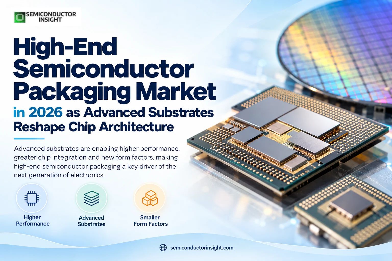
High-End Semiconductor Packaging Market in 2026 as Advanced Substrates Reshape Chip Architecture
Advanced semiconductor packaging is becoming a critical part of chip design, not simply the final step before a processor reaches a circuit board. As AI accelerators combine computing dies, high-bandwidth memory and increasingly dense interconnections, packaging determines how effectively these components work together.
High-end semiconductor packaging market is therefore moving toward architectures that improve bandwidth, power efficiency and system performance without relying exclusively on smaller transistors.
When the Package Becomes Part of the Processor
- Traditional packaging primarily protected chips and connected them to electronic systems.
- Today’s high-performance devices require a more integrated approach. Multiple dies can be placed side by side or stacked vertically, allowing processors, memory and specialised functions to communicate over shorter distances.
- This shift is especially relevant to AI servers, high-performance computing systems and advanced networking equipment.
- Rather than manufacturing every function on one large die, designers can combine specialised chiplets within a single package.
- This approach can improve design flexibility and help manufacturers manage the cost and yield implications of increasingly complex chips.
The HBM Connection Is Changing Package Design
High-bandwidth memory has become central to the architecture of advanced AI processors. Keeping large quantities of data close to computing units requires dense connections between logic dies and stacked memory, making package design a performance consideration rather than a secondary engineering decision.
- Samsung’s HBM4 announcement illustrates the direction of travel. Its published specifications describe a 12-layer HBM4 product with a 24-gigabit-per-second data rate per pin.
- The company has also outlined an HBM4E configuration with up to 64 GB of capacity and 4 TB/s of bandwidth in a 16-high stack. These examples demonstrate how memory density and package integration are evolving together.
Hybrid Bonding Moves Interconnects Closer Together
Hybrid bonding is attracting attention because it can connect dies through closely spaced copper and dielectric interfaces. Compared with conventional micro-bump approaches, this technique can support finer-pitch interconnections and more compact three-dimensional integration.
The implications extend beyond simply stacking more silicon. Shorter interconnect distances can help reduce parasitic effects and support dense communication between memory and logic. However, manufacturing requires precise surface preparation, alignment, bonding and defect control. Yield management will remain important as manufacturers move toward more demanding integration designs.
Glass Substrates Enter the AI Packaging Conversation
- As packages become larger and more complex, conventional substrate materials face increasing engineering demands. Glass is being explored for its dimensional stability, surface flatness and potential to support finer interconnect structures.
- In July 2026, Intel and Lens Technology announced a collaboration to explore glass-substrate packaging for future AI and data-centre workloads. T
- he initiative brings together semiconductor packaging expertise and precision glass processing. It highlights the importance of materials partnerships as manufacturers work on larger packages and higher interconnect densities.
- Glass is not an immediate replacement for every existing substrate. Production readiness, manufacturing cost, reliability and compatibility with established processes will influence how quickly the technology gains adoption.
New Manufacturing Capacity Is Following the Technology
Advanced packaging expansion is becoming a supply-chain priority. On September 8, 2026, Amkor announced a second phase of its Arizona packaging and test campus. The planned expansion adds 60,000 square metres of cleanroom space, bringing the proposed campus total to approximately 93,000 square metres and the planned investment to around $12 billion.
The project reflects a broader effort to establish advanced packaging capacity closer to semiconductor design and manufacturing customers. It also illustrates how packaging decisions increasingly involve manufacturing location, customer commitments and supply-chain resilience not only process technology.
Optical Links Could Change What Goes Inside a Package
- AI infrastructure depends on moving data between processors, memory and networking equipment at increasing speeds.
- Copper interconnects remain essential, but power consumption and signal constraints are encouraging development of optical connectivity closer to the computing package.
- Co-packaged optics combines optical components with electronic switching or computing systems to support high-bandwidth communication.
- TSMC’s published 3DFabric roadmap includes development of a compact silicon-photonics engine for integration with advanced packaging.
- Adoption will depend on cost, thermal management, assembly complexity and serviceability, but the technology could influence future AI networking designs.
The Next Packaging Breakthrough Will Need More Than Smaller Features
High-end semiconductor packaging market is evolving through the interaction of chiplets, stacked memory, hybrid bonding, new substrate materials and optical connectivity. Each technology addresses a different part of the same problem: delivering more computing capability within practical limits on power, space, manufacturing yield and cost.
The companies best positioned to advance these architectures will need to coordinate chip design, materials science, process equipment, assembly and testing. As AI systems grow more complex, the package is becoming a defining element of semiconductor performance rather than a finishing step.

Comments (0)