Future of Wafer Bonding Equipment: Key Opportunities & Challenges
Wafer Bonding Equipment Overview
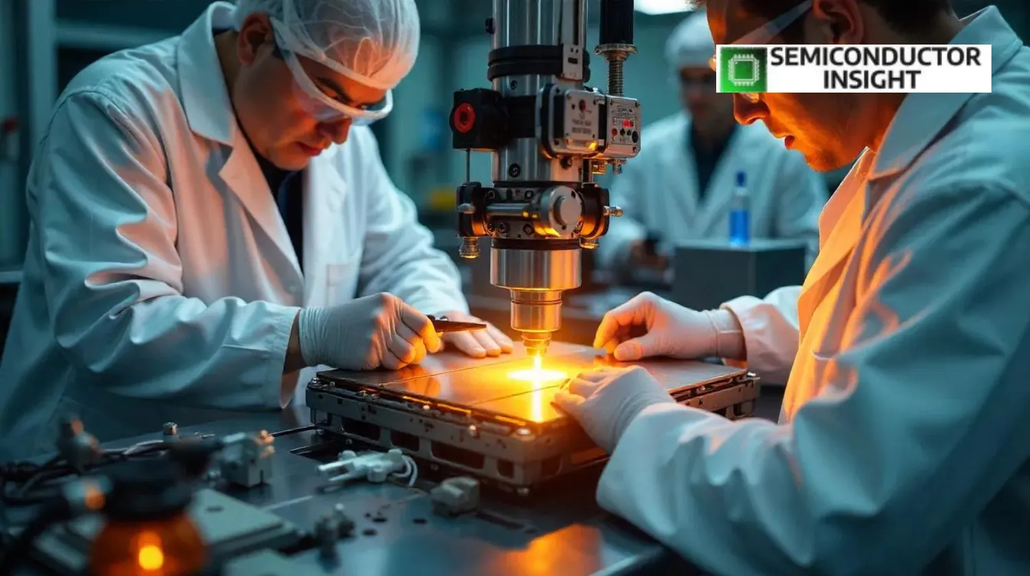
Wafer bonding equipment is a critical component in the semiconductor industry, enabling the fusion of multiple semiconductor wafers to create advanced microelectronic devices. As semiconductor technology continues to evolve, wafer bonding becomes increasingly important for producing high-performance devices with enhanced capabilities. This includes applications in 3D integrated circuits, micro-electromechanical systems (MEMS), power devices, and photonic devices.
In today’s competitive and rapidly evolving market, wafer bonding equipment has become essential for meeting the growing demand for smaller, faster, and more efficient electronic products. Industries such as telecommunications, automotive, consumer electronics, and renewable energy are particularly benefiting from the advancements in wafer bonding technologies.
Wafer Bonding Equipment Market Analysis
Market Size, Share, and Growth
The global wafer bonding equipment market has witnessed steady growth in recent years, driven by technological advancements and the increasing demand for high-performance semiconductor devices. In 2023, the market was valued at approximately $X billion and is expected to grow at a compound annual growth rate (CAGR) of 7-9% through 2032. As new applications emerge, particularly in fields such as 5G, AI, and IoT, the demand for more advanced wafer bonding solutions continues to rise.
The market’s growth is fueled by the need for next-generation microchips and components, with industries pushing for higher integration and miniaturization. Moreover, the ongoing evolution of 3D ICs, MEMS, and microelectronics in general is contributing to the increasing demand for wafer bonding equipment.
To dive deeper into the current trends and data,
Market Growth
The wafer bonding equipment market has significant growth potential, driven by key technological advancements and innovations in semiconductor manufacturing. With the rapid deployment of 5G technology, the automotive industry’s shift toward electric vehicles (EVs), and the rising demand for IoT devices, wafer bonding equipment is crucial to enabling smaller, faster, and more energy-efficient microchips.
Emerging applications like 3D semiconductor integration and MEMS devices will further fuel the market’s growth. The market is also witnessing a surge in investments, especially in Asia-Pacific and North America, where semiconductor production and R&D activities are heavily concentrated.
Key Applications or Uses of Wafer Bonding Equipment
Wafer bonding equipment is used across multiple industries and applications where high precision and reliability are paramount. Some of the most significant applications include:
- Semiconductor Manufacturing: The most common use of wafer bonding equipment is in semiconductor manufacturing, particularly in the creation of advanced 3D integrated circuits (3D ICs). These devices are critical in providing the required performance for next-generation mobile devices, computers, and data centers.
- MEMS (Micro-Electro-Mechanical Systems): MEMS devices are used in a wide range of applications, including sensors, actuators, and accelerometers. Wafer bonding plays a crucial role in integrating MEMS components to create these small, intricate devices that are now widely used in automotive, healthcare, and consumer electronics.
- LEDs and Photonics: In optoelectronics, wafer bonding equipment is essential for producing high-performance light-emitting diodes (LEDs) and photonic devices. Wafer bonding allows for efficient stacking and integration of semiconductor materials used in lighting, display technologies, and fiber optics.
- Solar Energy: Wafer bonding is used in the photovoltaic (solar) industry to enhance the efficiency and performance of solar cells. By enabling the bonding of different semiconductor materials, manufacturers can achieve better energy conversion rates.
Emerging Trends or Industry Analysis
The wafer bonding equipment market is continuously evolving, driven by several emerging trends and innovations:
- 3D IC Integration: The push for miniaturization in the semiconductor industry has led to the increased adoption of 3D IC technology. Wafer bonding is crucial for creating these multi-layered, highly integrated semiconductor devices, which offer improved performance, reduced size, and enhanced functionality.
- Hybrid and Direct Bonding Techniques: Advancements in wafer bonding technologies, including hybrid bonding and direct bonding methods, are gaining traction. These techniques allow for higher precision and better yield rates, particularly for 3D ICs and MEMS devices. They are expected to drive the next phase of growth in the wafer bonding equipment market.
- Increased Focus on Energy-Efficiency: As industries and consumers become more environmentally conscious, there is a growing demand for energy-efficient semiconductor devices. Wafer bonding technology has evolved to meet these demands by reducing energy consumption in manufacturing processes and enabling the production of energy-efficient devices.
- Automation and AI Integration: The integration of artificial intelligence (AI) and automation into wafer bonding processes is another growing trend. These innovations allow for faster and more accurate production, reducing the risk of errors and improving the efficiency of semiconductor manufacturing.
For further insights into these emerging trends and more,
Key Players in the Wafer Bonding Equipment Market
Several key players dominate the wafer bonding equipment market, driving its technological advancements and growth:
- EV Group (EVG): A leading provider of wafer bonding equipment, EVG is known for its innovative solutions in 3D IC integration, MEMS devices, and advanced packaging.
- SUSS MicroTec: A major player in the wafer bonding space, SUSS MicroTec offers a wide range of equipment for semiconductor manufacturing, particularly for MEMS, sensors, and power devices.
- Tokyo Electron Limited (TEL): TEL is a well-established semiconductor equipment manufacturer, providing advanced wafer bonding solutions for a variety of applications, including 3D ICs and MEMS.
- Applied Materials: Applied Materials is a global leader in materials engineering, offering cutting-edge wafer bonding technologies that are essential in semiconductor manufacturing.
Regional Insights
The wafer bonding equipment market is geographically diverse, with strong growth seen across key regions:
- Asia-Pacific: This region, particularly China, Japan, and South Korea, dominates the wafer bonding equipment market, as it is home to some of the world’s largest semiconductor manufacturers. The growing demand for advanced microelectronics in these countries will continue to propel the market.
- North America: The United States, with its strong focus on semiconductor innovation and R&D, is another major market for wafer bonding equipment. The demand for advanced semiconductor solutions in industries such as 5G, AI, and automotive will further boost market growth.
- Europe: Europe is also a growing market, with countries like Germany and France driving advancements in semiconductor manufacturing and MEMS device production.
Market Forecast
Looking ahead, the wafer bonding equipment market is expected to continue its upward trajectory through 2032. With a projected CAGR of 7-9%, the market will likely be valued at $X billion by 2032. As demand for smaller, more efficient devices grows, wafer bonding technology will play a pivotal role in meeting these requirements.
Prices for wafer bonding equipment are expected to stabilize, though technological advancements and increasing competition may lead to more affordable solutions. The ongoing integration of AI, automation, and energy-efficient technologies into wafer bonding processes is expected to drive significant innovation in the coming years.
Future Growth Opportunities
There are several key growth opportunities for the wafer bonding equipment market:
- Expansion in Emerging Markets: As demand for electronic devices grows globally, emerging markets in Southeast Asia, Latin America, and Africa present significant opportunities for wafer bonding equipment manufacturers.
- Growth in 5G and AI: The rollout of 5G networks and the widespread adoption of AI technologies are expected to drive the demand for more advanced semiconductor devices, creating new opportunities for wafer bonding equipment manufacturers.
- Sustainability Focus: As companies shift toward sustainable manufacturing processes, there is a growing demand for wafer bonding equipment that minimizes energy consumption and waste, opening doors for eco-friendly innovations.
Conclusion
The wafer bonding equipment market is positioned for significant growth in the coming years, driven by the increasing demand for advanced semiconductor devices and innovations in wafer bonding technologies. While challenges like technological complexity and the need for high precision remain, the opportunities for growth are abundant, particularly in 5G, AI, MEMS, and energy-efficient applications.
To stay ahead of the curve and explore the latest market trends,
FAQs
Q: What are the key applications of wafer bonding equipment?
A: Wafer bonding equipment is primarily used in semiconductor manufacturing, MEMS devices, LEDs, photonics, and solar energy applications.
Q: What is driving the growth of the wafer bonding equipment market?
A: The growth is driven by advancements in 3D IC integration, the rise of emerging technologies like 5G and AI, and the increasing demand for miniaturized and high-performance devices.
Q: What are the key players in the wafer bonding equipment market?
A: Major players in the market include EV Group (EVG), SUSS MicroTec, Tokyo Electron Limited (TEL), and Applied Materials.
Shubham K
Shubham is a seasoned market researcher specializing in the semiconductor industry, providing in-depth analysis on emerging trends, technological advancements, and market dynamics. With extensive experience in semiconductor manufacturing, supply chain analysis, and competitive intelligence, Shubham delivers actionable insights that help businesses navigate the evolving landscape of chip design, fabrication, and applications. His expertise spans key areas such as AI-driven semiconductors, advanced packaging, memory technologies, and foundry trends. At SemiconductorInsight, Shubham combines data-driven research with strategic foresight, offering thought leadership that empowers industry professionals, investors, and technology innovators to make informed decisions.
Comments (0)