
From Design to Silicon Photomask Market Connection
A microscopic foundation of modern chips
When people talk about semiconductors, the spotlight usually falls on chips, fabs, or cutting-edge nodes. Rarely does attention shift to the thin, almost invisible component that quietly defines how circuits are etched onto silicon the photomask. In 2026, photomask market has become a critical pillar in semiconductor manufacturing, acting as the blueprint carrier for every transistor pattern printed during lithography.
A photomask is essentially a quartz plate embedded with intricate circuit patterns. During lithography, light passes through this mask to transfer patterns onto a silicon wafer. What sounds straightforward becomes extraordinarily complex at advanced nodes, where even a nanometre-level defect can disrupt performance.
For additional report info, feel free to view our most related recent edition: https://semiconductorinsight.com/report/logic-ic-photomask-market/
Where precision meets physics
At its core, the photomask process sits at the intersection of optics, materials science, and nanotechnology. With chipmakers now operating at nodes below 5 nm, the demand for defect-free masks has intensified dramatically.
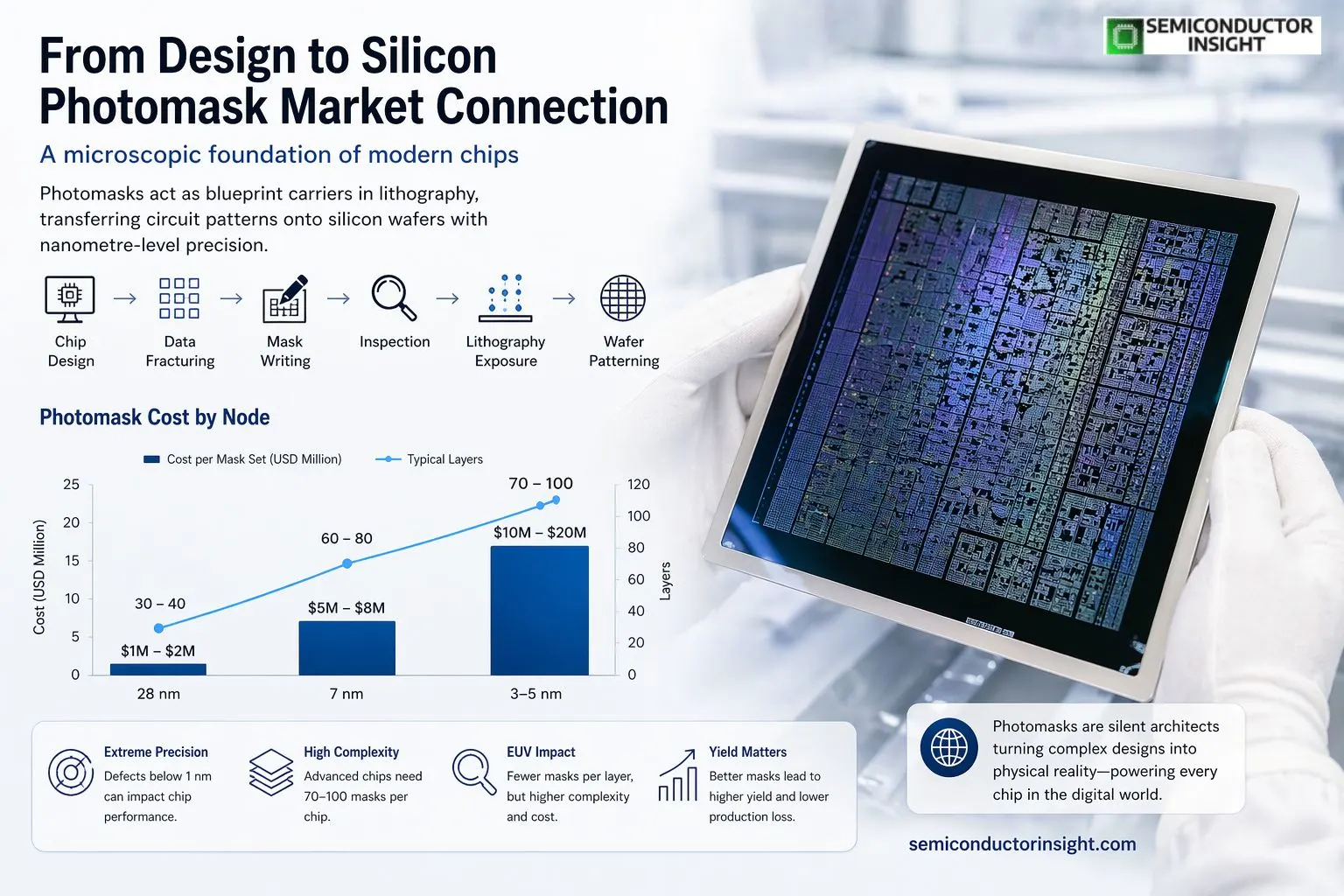
Chip Design → Data Fracturing → Mask Writing → Inspection → Lithography Exposure → Wafer Patterning
Each step requires extreme accuracy. For example, mask writing systems today operate with electron beams that can define features smaller than 10 nanometers. Even a single mask set for an advanced processor can include 70 to 100 individual masks, each representing a different layer of the chip.
The cost narrative that is reshaping decisions
Photomasks are no longer just technical components; they have become significant cost drivers in semiconductor production. For advanced nodes, a full mask set can cost anywhere between $10 million to $20 million, depending on complexity and layer count. This has forced chip designers to rethink how they approach product development, especially for low-volume or specialized chips.
- Photomask costs continue to rise as semiconductor nodes become more advanced and production requirements grow more complex.
- At the 28 nm node, a typical mask set costs around $1 million to $2 million, with 30 to 40 layers.
- For the 7 nm node, costs increase significantly to about $5 million to $8 million, while the number of layers rises to 60 to 80.
- At the 3 to 5 nm level, mask set costs can reach $10 million to $20 million, with around 70 to 100 layers.
- This sharp increase in cost has encouraged the adoption of multi-patterning reduction techniques and greater use of simulation tools to reduce mask revisions and improve efficiency.
EUV adoption rewriting the rules
The introduction of Extreme Ultraviolet lithography has significantly changed the photomask landscape. EUV masks are far more complex than traditional ones, requiring reflective multilayer structures instead of transparent quartz-based designs.
In 2026, EUV mask production is still limited to a handful of specialized facilities globally, which adds to supply constraints. Each EUV mask undergoes rigorous defect inspection using advanced actinic inspection systems tools that operate at the same wavelength used in actual lithography.
Interestingly, EUV masks have reduced the number of masks required per chip layer in some cases, but the complexity and cost per mask have increased, balancing out the overall economics.
Data intensity and yield precision shaping modern photomasks
One of the more understated yet transformative shifts in the photomask landscape is the explosion of data complexity and its direct connection to manufacturing yield. As chip architectures become denser and more intricate, the data required to design a single photomask has expanded dramatically.
- Today, advanced mask files often run into terabytes, demanding high-performance computing systems just to process, fracture, and verify the patterns before production even begins.
- This has pushed the industry toward highly specialized software ecosystems built around mask data preparation, proximity correction algorithms, and predictive simulation tools.
- Engineers now spend a significant portion of the development cycle refining these digital layouts, ensuring that what gets printed on silicon is as close to perfection as possible.
- This growing data intensity is not just a technical challenge it plays a critical role in determining production efficiency.
- Photomask quality has a direct and amplified impact on yield, which refers to the number of functional chips produced from each wafer.
- Even the smallest defect on a mask can replicate across thousands of chips, turning a minor imperfection into a large-scale manufacturing loss.
To address this, manufacturers are investing heavily in next-generation inspection systems capable of detecting defects at near-atomic scales. By 2026, some of these systems can identify anomalies smaller than 1 nanometre, significantly improving consistency across production batches. In this environment, the relationship between data precision and yield performance has become inseparable, making photomask optimization as much a digital challenge as it is a physical one.
The evolving craftsmanship behind photomasks
Despite being a highly technical field, photomask manufacturing still involves a level of craftsmanship. Engineers fine-tune parameters, adjust exposure techniques, and continuously refine processes to achieve near-perfect results.
What makes this market fascinating is that it operates behind the scenes, yet directly influences the performance of everything from smartphones to supercomputers. As semiconductor devices continue to evolve, photomask market remains deeply embedded in that journey quietly enabling every leap forward.
In many ways, photomasks are not just tools but silent architects of the digital world, translating complex designs into physical reality with unmatched precision.

Comments (0)