

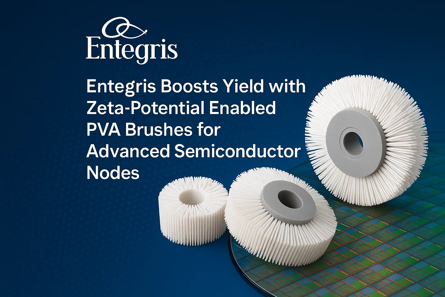
Entegris Boosts Yield with Zeta-Potential Enabled PVA Brushes for Advanced Semiconductor Nodes
In the highly intricate world of semiconductor fabrication, Chemical Mechanical Planarization (CMP) is an indispensable step that ensures surface uniformity critical for multilayer device structures. However, an often-understated component in this process is the Post-CMP cleaning stage, which relies heavily on Polyvinyl Alcohol (PVA) brushes. These specialized brushes are crucial in removing residual slurry, particles, and contamination without damaging the delicate wafer surface. The post-CMP PVA brush market, long considered a technical niche, is now experiencing a significant surge in innovation, demand, and strategic importance.
As of 2024, the Post-CMP PVA Brush Market was valued at US$ 312.4 million and is projected to grow steadily to US$ 498.7 million by 2032, representing a robust CAGR of 6.87% over the forecast period.
Access Your Free Sample Report- Post CMP PVA Brush Market
- The Role of Post-CMP Cleaning in Semiconductor Manufacturing
After the CMP process, which uses a combination of chemical and mechanical forces to planarize wafer surfaces, microscopic particles and slurry residues remain. If not adequately removed, these contaminants can lead to circuit defects, reduced yield, and reliability issues in the final semiconductor device. This is where PVA brushes come in. These brushes, made from porous, hydrophilic polyvinyl alcohol material, gently clean the wafer surface without scratching or causing damage.
Advanced post-CMP cleaning systems often employ a combination of PVA brushes, DI (deionized) water, and chemical cleaning solutions. The brushes’ open-pore structure allows effective particle trapping while enabling chemical diffusion, providing a superior cleaning performance that’s vital for advanced nodes (7nm and below).
- Technological Innovations in PVA Brushes
Recent developments in PVA brush design and manufacturing are driven by the increasing complexity of semiconductor devices and the push toward smaller nodes and 3D architectures:
2.1 Ultra-Fine Fiber Structures:
Around 28% of newly launched PVA brushes now incorporate ultra-fine fibers that significantly improve the removal of sub-50nm particles. These structures are designed to interact more effectively with wafer surfaces, delivering a higher particle removal efficiency (PRE) without increasing surface roughness.
2.2 Sensor-Integrated Brushes:
Smart manufacturing and Industry 4.0 principles are making their way into the cleanroom. Some newer brush systems now incorporate embedded sensors to monitor brush wear, contact force, and cleaning effectiveness in real-time. This allows predictive maintenance, reducing wafer loss due to tool errors and improving uptime.
2.3 Precision Pore Engineering:
Brushes are now being manufactured with engineered porosity gradients—larger pores on the outer layers for higher slurry uptake and finer pores near the surface for effective particle scrubbing. This dual-porosity approach improves cleaning while reducing brush replacement frequency.
2.4 Compatibility with Advanced Chemistries:
Modern nodes require chemical formulations tailored to exotic materials such as cobalt, ruthenium, or low-k dielectrics. PVA brushes are now being developed with enhanced chemical compatibility coatings to resist degradation from aggressive post-CMP chemicals.
- Sustainability and Environmental Responsibility
Sustainability is becoming a major driver in fab operations. PVA brush manufacturers are responding with a range of innovations that minimize waste and environmental impact:
3.1 Recyclable Materials:
Approximately 19% of new PVA brushes now use recyclable PVA formulations or support closed-loop recycling programs within fabs. These options help reduce polymer waste and support fabs’ carbon reduction goals.
3.2 Longer Brush Life:
By improving durability and anti-fouling coatings, the brush lifespan has increased by 15–20%, reducing overall material consumption and downtime for brush changes.
3.3 Reduced Water and Chemical Use:
Advanced brush designs now improve cleaning performance per unit of chemical used, enabling fabs to reduce deionized water and cleaner usage. This is especially critical in water-scarce regions like Taiwan or Arizona.
Download Sample Report PDF- Post CMP PVA Brush Market
- Regional Dynamics: Global Market Developments
4.1 North America’s Technological Edge:
The United States has emerged as a key player in post-CMP brush innovation. Major U.S. fabs and toolmakers now contribute to over 23% of global production. Notably, over 32% of advanced wafer-cleaning solutions used globally are sourced from U.S.-based suppliers. Federal support for chip manufacturing under the CHIPS Act has further accelerated domestic R&D in post-CMP processes.
4.2 Asia Pacific Dominance:
Despite the innovation boom in the West, Asia-Pacific remains the epicenter of demand. Countries like Taiwan, South Korea, and China collectively account for over 50% of global brush usage. With TSMC, Samsung, and SMIC expanding 3nm and 2nm process nodes, the demand for ultra-clean wafer surfaces has never been higher.
4.3 Europe’s Green Manufacturing Leadership:
European semiconductor companies are pushing for greener fabrication solutions, driving demand for eco-friendly PVA brushes. Sustainability regulations in the EU are pushing fabs to opt for recyclable brush technologies and water-saving cleaning methods.
- Market Outlook and Growth Trajectory
5.1 Growth Forecast (2025–2032):
With the Post-CMP PVA Brush Market poised to grow from US$ 312.4 million in 2024 to US$ 498.7 million by 2032 at a CAGR of 6.87%, the market outlook remains robust. Growth is driven not only by increased chip production but also by the higher frequency of cleaning required in smaller process nodes and complex 3D structures.
5.2 Demand by Segment:
- Logic Devices (37%): Particularly for FinFET and Gate-All-Around (GAA) nodes, requiring high-purity cleaning.
- Memory (28%): 3D NAND and DRAM lines where stacked layers necessitate rigorous surface planarization and cleaning.
- Foundries (24%): As contract manufacturers take on varied device nodes, cleaning solutions must be adaptable and efficient.
- Analog & Others (11%): Includes MEMS and power devices requiring selective cleaning strategies.
5.3 Competitive Landscape:
Key players are intensifying innovation through collaborations with fab tool OEMs. The push for localized manufacturing—especially in the U.S. and India—is also driving regional supply chain diversification.
- Challenges and Opportunities
6.1 Supply Chain Vulnerabilities:
Geopolitical tensions and logistical constraints (e.g., shipping delays and polymer shortages) remain key risks. Building resilient regional supply chains for PVA brush components will be crucial.
6.2 Customization Needs:
As device architectures diverge, no one-size-fits-all solution exists for post-CMP cleaning. Brush manufacturers must increasingly co-develop application-specific solutions with semiconductor fabs.
6.3 Automation and Smart Integration:
There is growing demand for PVA brush systems that integrate seamlessly with fab-wide automation, enabling real-time defect tracking and adaptive process control.
6.4 Sustainability Standards:
Stricter environmental regulations are both a challenge and an opportunity. Manufacturers who can meet or exceed sustainability benchmarks will gain a competitive edge.
- Future Trends
7.1 AI-Driven Brush Monitoring:
Future systems will likely incorporate AI to predict brush degradation and optimize cleaning cycles autonomously.
7.2 Hybrid Cleaning Systems:
Emerging techniques are integrating PVA brushes with megasonic or UV cleaning to enhance particle removal while lowering chemical usage.
7.3 Localized Manufacturing Hubs:
To mitigate geopolitical risks, fabs are investing in localized brush production facilities, especially in North America and Southeast Asia.
7.4 Circular Economy Initiatives:
New programs are exploring refurbishing used PVA brushes through controlled reprocessing, enabling circular material use within fabs.
Click Here To Download Full Sample Report- Post CMP PVA Brush Market
As semiconductor nodes shrink and performance demands grow, the seemingly humble PVA brush has become a linchpin in achieving high device yield and reliability. With technological innovations, sustainability enhancements, and increasing integration into smart manufacturing ecosystems, the post-CMP PVA brush market is evolving from a support function into a critical enabler of next-generation chip fabrication.
Driven by a forecasted CAGR of 6.87%, the market’s growth story is underpinned by both necessity and opportunity. Whether it’s ultra-fine pore brushes cleaning 2nm wafers or sensor-equipped systems enabling Industry 4.0 in fabs, the future is being polished—one wafer at a time.

Comments (0)