
ENEPIG Process Market Trends Elevate Packaging Performance and Longevity
In modern semiconductor manufacturing, the reliability of a device often depends on what cannot be seen the chemistry of its surface finishes. As packages become smaller, interconnect density increases, and devices operate under harsher thermal and electrical conditions, traditional surface finishing solutions face performance limitations. This is where the ENEPIG (Electroless Nickel Electroless Palladium Immersion Gold) process has emerged as a preferred choice for advanced semiconductor packaging.
The ENEPIG process is not simply an incremental improvement over older finishes; it represents a strategic shift toward multi-metal, chemically engineered surface layers that enhance solder ability, wire bonding reliability, and long-term corrosion resistance.
For a more thorough report, please contact us using our most recent report:
https://semiconductorinsight.com/report/enepig-process-market/
Defining the ENEPIG Process in Semiconductor Manufacturing
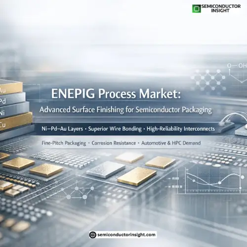
ENEPIG is a three-layer surface finish applied to copper pads and traces. It consists of an electroless nickel base layer, a thin electroless palladium barrier, and an immersion gold top layer. Each layer performs a distinct function, working together to protect copper surfaces and ensure reliable electrical connections.
What differentiates ENEPIG from earlier finishes is the palladium interlayer, which acts as a diffusion barrier and significantly improves performance during both soldering and wire bonding. This makes ENEPIG especially suitable for fine-pitch, high-density semiconductor packages where consistency and reliability are critical.
Why ENEPIG Is Gaining Market Preference?
The growing adoption of ENEPIG is closely tied to changes in semiconductor design and packaging architecture. Devices used in automotive electronics, data centres, medical equipment, and industrial automation demand longer lifecycles and higher thermal stability.
In comparison to conventional ENIG finishes, ENEPIG reduces issues such as nickel corrosion, black pad formation, and brittle intermetallic compounds. Industry studies indicate that ENEPIG-finished pads can demonstrate up to 30-40% improvement in wire bond pull strength consistency, particularly in gold and copper wire bonding applications.
Chemical Engineering behind the ENEPIG Process
From a chemical perspective, ENEPIG relies on precise bath chemistry control and sequential deposition reactions. The electroless nickel layer provides mechanical strength and acts as a diffusion barrier against copper migration. The palladium layer typically only a few tenths of a micron thick prevents nickel oxidation and improves bonding compatibility.
The immersion gold layer protects the underlying metals from oxidation during storage and handling. Although extremely thin, it plays a critical role in maintaining surface integrity prior to assembly. The success of the ENEPIG process depends on bath stability, metal ion concentration, pH control, and temperature management, making it a chemistry-intensive surface finishing method.
Semiconductor Packaging Applications Driving Demand
ENEPIG is increasingly used across a range of semiconductor packaging formats, including ball grid arrays (BGAs), chip-scale packages (CSPs), system-in-package (SiP), and advanced substrate technologies. As package geometries shrink, the tolerance for surface defects narrows, pushing manufacturers toward finishes that deliver uniform thickness and predictable performance.
In advanced packaging lines, ENEPIG adoption has grown steadily, with industry estimates suggesting that over 20% of high-density substrate finishes now utilize ENEPIG, particularly in applications requiring mixed wire bonding and soldering processes.
Market Momentum across End-Use Industries
The ENEPIG process market benefits from strong pull across multiple end-use sectors. Automotive electronics, where reliability standards are stringent, increasingly specify ENEPIG for control units, sensors, and power management modules. Similarly, high-performance computing and networking equipment rely on ENEPIG to support high-frequency signal integrity and thermal cycling durability.
Consumer electronics manufacturers are also turning to ENEPIG for premium devices, especially where ultra-fine interconnects and compact designs demand consistent surface chemistry across large production volumes.
Global Production Trends and Regional Adoption
Asia-Pacific remains the dominant region for ENEPIG process adoption, driven by semiconductor fabrication and substrate manufacturing hubs in China, Taiwan, South Korea, and Japan. These regions account for an estimated 60% or more of global ENEPIG surface finishing activity, supported by mature chemical supply chains and advanced plating infrastructure.
North America and Europe continue to adopt ENEPIG in specialized and high-reliability applications, particularly in aerospace, defence, and medical electronics. In these markets, ENEPIG is valued for its process stability and long-term performance rather than cost optimization alone.
Cost Structure and Process Economics
While ENEPIG involves higher material costs than traditional finishes due to palladium usage, manufacturers increasingly view it as a value-driven investment rather than an expense. The reduction in rework, scrap rates, and field failures often offsets higher upfront costs.
In production environments, ENEPIG has been shown to reduce defect-related yield losses by up to 15% in complex assemblies, making it economically attractive for advanced packaging lines where failure costs are high.
Regulatory and Quality Compliance Considerations
ENEPIG processes align well with global environmental and safety standards, including RoHS and REACH compliance, due to the absence of lead and controlled use of heavy metals. Chemical suppliers continue to refine formulations to reduce waste generation and improve bath longevity, supporting sustainability goals within semiconductor manufacturing.
Quality control protocols emphasize thickness uniformity, surface roughness, and chemical purity, all of which are critical for meeting stringent semiconductor reliability requirements.
Competitive Landscape and Process Innovation
ENEPIG process market is shaped by collaboration between specialty chemical suppliers, plating equipment manufacturers, and semiconductor fabricators. Continuous innovation focuses on improving palladium utilization efficiency, stabilizing bath chemistry, and enabling finer pitch compatibility.
Recent developments include low-palladium ENEPIG formulations and enhanced process monitoring tools that improve repeatability across high-volume manufacturing environments.
As semiconductor devices continue to evolve toward higher integration, smaller form factors, and longer service life, surface finishing technologies will play an increasingly strategic role. ENEPIG stands out as a solution that bridges chemical precision and semiconductor performance, enabling manufacturers to meet the demands of next-generation electronics.
ENEPIG process market is therefore positioned not merely as a niche finishing technique, but as a critical enabler of advanced semiconductor packaging reliability and scalability.

Comments (0)