
Why Electro-Optic Laser Power Stabilization System Market Are Becoming Essential in Semiconductor Lithography?
Modern semiconductor manufacturing relies heavily on stable laser performance. Electro-optic laser power stabilization systems ensure that lasers maintain a constant optical output during complex fabrication steps such as lithography, wafer inspection and metrology. As chip geometries shrink and manufacturing tolerances tighten, even minor fluctuations in laser intensity can lead to pattern defects or measurement errors.
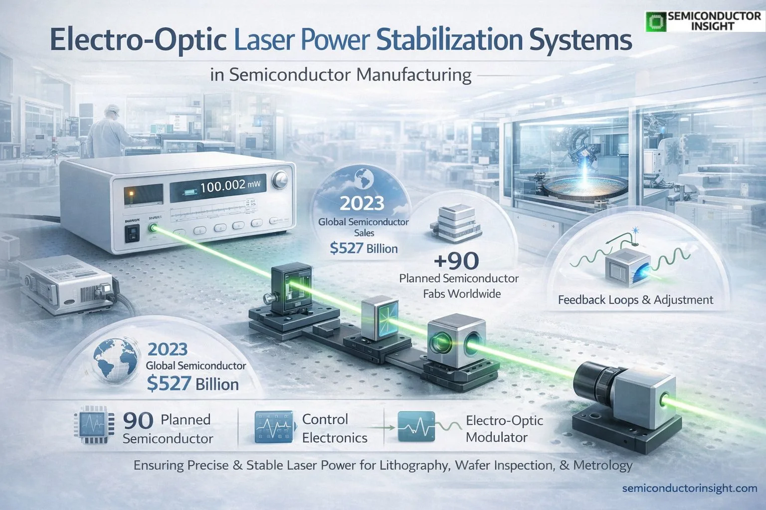
The amount of semiconductors that can be made around the world is still growing quickly. The Semiconductor Industry Association states that global semiconductor sales hit USD 527 billion in 2023. This shows how big chip production facilities are all over the world. Each advanced fabrication factory has hundreds of optical measuring and lithography equipment, and many of them need lasers that are very stable to work properly.
Electro-optic stabilization technology works by adjusting the intensity of a laser beam through feedback loops that detect and correct fluctuations in real time. This ability to maintain laser stability at extremely precise levels makes these systems essential for semiconductor manufacturing tools operating at nanometer-scale precision.
Laser Stability Requirements in Advanced Lithography Systems
Lithography tools used in semiconductor fabrication are among the most sophisticated optical systems ever built. Deep ultraviolet (DUV) and extreme ultraviolet (EUV) lithography rely on laser-driven plasma sources and precision optical feedback mechanisms. In these environments, power fluctuations measured in milliwatts can influence pattern resolution across entire wafers.
Industry reports from equipment manufacturers highlight the scale of lithography deployment. One leading semiconductor equipment provider reported shipping over 400 lithography systems globally in a single year, each designed to process thousands of wafers monthly. Maintaining consistent optical power during these processes requires advanced stabilization modules capable of responding to rapid intensity changes within microseconds.
The growing complexity of semiconductor nodes further increases the need for stabilized optical systems. Chips manufactured at 3-nanometer and 5-nanometer nodes require tighter exposure control than earlier generations, making stabilization systems a critical component of the lithography ecosystem.
Please Take a Look at Our Updated Report before Continuing: https://semiconductorinsight.com/report/electro-optic-laser-power-stabilization-system-market/
Integration with Semiconductor Metrology and Inspection Tools
Beyond lithography, electro-optic stabilization systems are widely used in semiconductor metrology. Optical inspection tools scan wafers for defects using laser beams with extremely controlled intensity levels. Any variation in beam power can distort measurement accuracy or reduce defect detection sensitivity.
Semiconductor fabrication facilities run inspection cycles continuously. A single advanced fabrication plant may process more than 40,000 wafer starts per month, and each wafer undergoes multiple optical inspection stages. Stabilized laser output allows these systems to detect nanometer-scale surface variations and microscopic defects during production.
Manufacturers of optical metrology equipment frequently integrate stabilization modules directly into their laser subsystems. These modules maintain constant beam output even when environmental factors such as temperature drift or electronic noise influence laser performance.
Growing Semiconductor Infrastructure and Optical Equipment Demand
The expansion of semiconductor infrastructure is driving the installation of advanced optical equipment. According to global semiconductor manufacturing data released by industry associations and government agencies, over 90 new semiconductor fabrication facilities are planned or under construction worldwide between 2022 and 2026.
Each fabrication facility contains a wide range of optical instruments used for wafer exposure, inspection, alignment, and measurement. These tools depend on stable light sources to maintain process accuracy during long production cycles that can run for 24 hours a day.
Government initiatives supporting semiconductor manufacturing are also accelerating equipment deployment. The United States’ CHIPS and Science Act allocates approx. USD 52 billion to support semiconductor manufacturing and research infrastructure. Similarly, Japan and South Korea have announced large-scale investments in advanced chip production facilities, further expanding demand for precision optical technologies.
Role in Optical Feedback Control and High-Precision Laser Systems
- Electro-optic stabilization systems play a central role in modern optical feedback architectures. These systems combine photodetectors, electro-optic modulators, and control electronics to regulate laser output with high speed and accuracy.
- In semiconductor processing environments, stabilized laser systems support multiple functions including wafer alignment, mask inspection, and interferometric measurement.
- Optical engineers emphasize that precision optics combined with stabilization feedback can maintain beam intensity fluctuations below a few parts per million, enabling reliable performance during long production cycles.
Scientific research laboratories and photonics development centers are also expanding the use of stabilized laser systems. National laboratories and university semiconductor research programs frequently rely on stabilized laser platforms for optical experiments involving nanoscale materials and photonic devices.
As semiconductor manufacturing continues to push the boundaries of miniaturization and optical precision, electro-optic laser power stabilization systems are becoming a foundational technology supporting the accuracy and reliability of next-generation chip fabrication.

Comments (0)