Copper Posts, AI Precision, and Eco-Friendly Reflow: How Solder Ball Mounting Equipment Is Powering the Next Generation of Semiconductor Packaging
The semiconductor industry is racing ahead, driven by the exponential demand for smaller, faster, and more power-efficient chips. As chip architecture evolves, so too must the equipment used in their packaging. Among these crucial tools, solder ball mounting equipment plays a silent but transformative role. This specialized machinery, essential for Ball Grid Array (BGA), flip-chip, and advanced system-in-package (SiP) assembly, is undergoing a quiet revolution—reshaping the future of semiconductor integration.
In 2024, the Solder Ball Mounting Equipment for Semiconductor Packaging Market was valued at USD 89.4 million. With ongoing innovation and market expansion, it is projected to grow to USD 149.3 million by 2032, exhibiting a compound annual growth rate (CAGR) of 6.7% over the forecast period (2025–2032).
Access Your Free Sample Report- Solder Ball Mounting Equipment for Semiconductor Packaging Market
Understanding Solder Ball Mounting: A Cornerstone of Semiconductor Packaging
Solder ball mounting is the process of depositing small spherical solder balls onto semiconductor packages to create electrical interconnects. These balls enable signal transmission from the chip to the PCB or another substrate. This technology is at the heart of BGA, CSP, WLCSP, and 3D IC assembly lines.
The increasing complexity of integrated circuits (ICs), from high-bandwidth memory (HBM) to heterogeneous chiplet packages, demands greater precision, speed, and defect-free placement in solder ball mounting equipment.
Recent Technological Developments: A New Era of Precision and Flexibility
- LG Innotek’s Copper Post Innovation: Solder Balls with a Twist
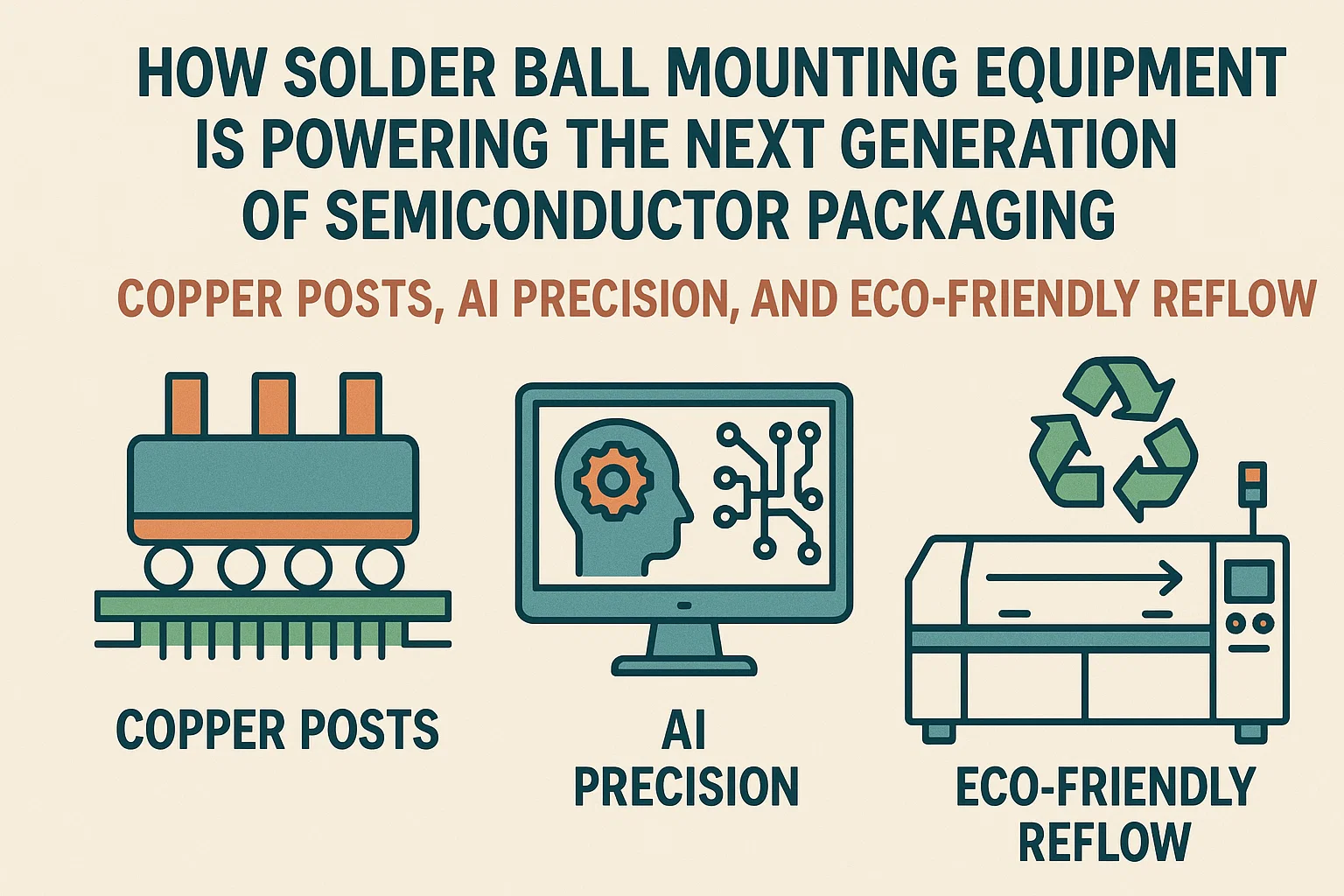
One of the most headline-grabbing innovations came from LG Innotek, which recently unveiled a hybrid approach: combining copper pillars topped with solder balls instead of relying on traditional solder ball-only structures. This innovation offers a tighter ball pitch—by about 20%—and drastically improves both thermal conductivity and mechanical robustness.
This shift is significant. Copper posts offer better heat dissipation and reduce electromigration risks, key for power-hungry devices such as AI chips and 5G RF modules. LG’s patented technology (with 40+ patents filed) is expected to be implemented in next-gen smartphones and wearables, making their designs slimmer and more thermally efficient.
Insight: This copper-solder hybrid technique may become the new standard in high-density packaging, pressuring traditional solder ball mounters to adapt.
- AI and Machine Learning for Enhanced Accuracy
Modern solder ball mounting machines now come equipped with AI-powered alignment algorithms and real-time error correction systems. These smart systems adjust ball placement dynamically, compensating for wafer warpage, contamination, or environmental changes.
By reducing defect rates by up to 88%, these intelligent systems ensure first-pass yield improvements, minimize costly rework, and enable predictive maintenance—key in 24/7 production environments. Companies are integrating closed-loop vision systems and multi-axis robotic arms to deliver placement accuracies of ±3–5 µm.
- Ultra-Fine Pitch Precision for Advanced Packaging
With chip interconnects shrinking, mounting solder balls of ≤100 µm pitch has become a necessity. Leading equipment now features:
- High-resolution optical alignment
- Laser-assisted ball pre-heating
- Temperature-controlled platforms
- Self-cleaning nozzles for continuous operation
These innovations cater to 3D-IC, chiplet, and SiP packaging, where tight pitch and low warpage are essential. For example, machines like the Accura Ball Attach System by Kulicke & Soffa can place solder balls as small as 50 µm, achieving first-pass yields of 98.7%.
- Modular Ball Feeders: Supporting Multiple Sizes in One Platform
OEMs now demand flexibility, especially in contract manufacturing environments. Responding to this, equipment vendors have introduced modular ball feeders that can handle ball diameters from 0.12 mm to 0.76 mm without hardware changeovers. This not only reduces downtime but also enables quick transitions between different packaging formats—critical for EMS providers supporting multiple customers.
- Flux-Free Ball Mounting Systems for Green Manufacturing
Environmental sustainability is reshaping how semiconductor packaging is approached. Traditional soldering methods rely heavily on flux, which introduces chemical residues requiring extensive post-cleaning. Newer ball mounting systems use flux-free vacuum reflow and plasma-assisted activation to clean surfaces before bonding.
These flux-less systems reduce environmental waste and improve package reliability, especially for aerospace, automotive, and medical applications where long-term reliability is non-negotiable.
Download Sample Report PDF- Solder Ball Mounting Equipment for Semiconductor Packaging Market
Leading Players and Strategic Moves: Who’s Winning the Race?
The solder ball mounting equipment market is competitive, with innovation-driven players leading the way.
- ASM Pacific Technology (ASMPT)
ASMPT remains a market leader with machines boasting micron-level accuracy, high UPH (units per hour), and in-line AOI (automated optical inspection). Their recent models integrate digital twin technology for virtual process optimization and error simulation.
Highlight: ASMPT machines are widely adopted for advanced memory packaging and chiplet assembly.
- Shinkawa Ltd.
A Japanese pioneer in ball-attach automation, Shinkawa specializes in laser heating systems and multi-site ball mounters. Their platforms support ultra-compact packages—popular in automotive semiconductors—while achieving <2% void rates even under high nitrogen environments.
Focus area: 3D NAND, automotive microcontrollers, and MEMS packaging.
- Kulicke & Soffa (K&S)
K&S continues to innovate with its Accura series, which supports ultra-fine pitch and high-accuracy solder ball placement. Their 2024 Q1 report revealed a 22% increase in orders related to advanced packaging tools, primarily driven by demand for HBM and heterogeneous integration.
Advantage: Smart analytics dashboards for process traceability and real-time monitoring.
- Hitachi High-Tech
Known for its hybrid solder/laser bonding systems, Hitachi caters to the defense and aerospace sectors, offering MIL-STD-certified platforms with solder ball size compatibility down to 10 µm. Their equipment supports multi-alloy interconnects, a rising trend in heterogeneous chip stacks.
- Emerging Players: Fastprint Circuit Tech
This Chinese manufacturer has carved out market share by offering cost-effective ball mounters targeting mid-tier manufacturers. Their platforms, while not as precise, are sufficient for standard BGA and LGA packaging and have gained traction in India, Southeast Asia, and Eastern Europe.
Market Drivers: Why the Growth?
- Explosion in Advanced Packaging
Markets like HBM, AI accelerators, chiplets, and heterogeneous integration are driving demand for ultra-precise solder ball mounters. With more dies packed into tighter spaces, interconnect accuracy has never been more critical.
- Automotive Electronics Surge
With EVs and ADAS systems rising rapidly, the automotive sector needs ruggedized and miniaturized packaging. Solder ball mounters capable of working with high-reliability lead-free alloys and automotive-grade packages are in increasing demand.
- Asia-Pacific Dominance
Asia-Pacific continues to lead the global packaging market, with Taiwan, China, South Korea, and Japan accounting for a lion’s share of packaging investments. Government-backed chip initiatives in India and Vietnam are also expected to spur localized demand for compact, affordable ball mounting solutions.
Challenges and Headwinds
- Supply Chain Instability
Global electronics manufacturing still faces supply chain bottlenecks, especially in sourcing precision optics, servo motors, and micro-controllers for ball attach machines. These challenges affect production timelines and cost structures.
- Training and Integration Complexity
Advanced solder ball machines require highly trained operators and precise cleanroom conditions. Integrating these machines into older lines without disrupting yield is a challenge for many legacy fabs.
Future Outlook: What Lies Ahead for 2025–2032?
With the global market expected to grow from $89.4 million in 2024 to $149.3 million by 2032, several trends are poised to shape its future:
| Year | Key Trend |
| 2025 | Adoption of AI-driven multi-site placement platforms |
| 2026 | Flux-less soldering becomes the new normal |
| 2027 | Rise in copper-post solder mounting due to thermal limits |
| 2028 | Expansion in India & Vietnam packaging fabs fuels demand |
| 2029 | Miniaturized, tabletop machines for low-volume high-mix |
| 2030 | Voice-activated, closed-loop systems with cloud diagnostics |
| 2031 | Integration with hybrid bonding and 3D stacking platforms |
| 2032 | Solderless interconnects begin emerging, but legacy persists |
Conclusion: A Vital Link in the Semiconductor Chain
Solder ball mounting equipment may not make the headlines like AI chips or lithography machines, but its role in the advanced packaging ecosystem is indispensable. As packaging shifts from being a passive protective layer to an active performance driver, the need for ultra-precise, smart, and eco-conscious ball mounting systems will only accelerate.
The coming decade will be defined by miniaturization, modularity, and automation. Companies that embrace innovation—whether through AI, eco-friendly materials, or hybrid interconnect techniques—will lead the charge in transforming semiconductor assembly for the next generation.
Comments (0)