China Stockpiles Used PVD Tools Amid Export Bans, Fuels Global Gray Market Surge
The global semiconductor industry is experiencing a renaissance, driven by explosive growth in artificial intelligence, high-performance computing, 5G deployment, and electric vehicles. At the heart of this transformation lies the indispensable role of fabrication equipment—and specifically, Physical Vapor Deposition (PVD) tools. As chipmakers scale down nodes and diversify fabrication locations, the market for used wafer PVD equipment is undergoing unprecedented growth and strategic shifts.
Valued at US$ 7.82 billion in 2024, the wafer used PVD equipment market is projected to nearly double to US$ 14.67 billion by 2032, growing at a CAGR of 9.4% during the 2025-2032 forecast period.
Access Your Free Sample Report- Wafer Used PVD Equipment Market
- The Technological Push: Scaling to Advanced Nodes with Used PVD Tools
The drive toward smaller process nodes has led to a new level of sophistication in deposition requirements. Applied Materials, a long-standing industry leader, recently announced the expansion of its Endura® platform, designed to support the increasingly complex interconnect structures needed for sub-2nm logic nodes.
While traditionally viewed as a domain dominated by new equipment, recent reports from Bloomberg and Reuters indicate that Applied Materials is also enhancing legacy and used systems with upgraded process kits and AI-driven diagnostics. These enhancements make older systems viable for foundries targeting advanced packaging and back-end-of-line (BEOL) processes. This is a significant shift—and a clear indication that used PVD equipment is no longer relegated to legacy node production alone.
Key Insight: Foundries now see value in hybridizing new tech with older tools. This not only reduces capital expenditure but aligns with sustainability goals.
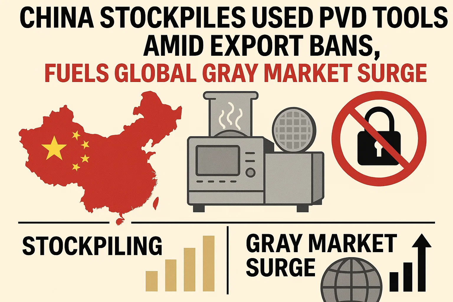
- Geopolitical Drivers: China, Export Restrictions, and the Grey Market Surge
One of the biggest catalysts in the used equipment boom is the ongoing US-China tech decoupling. With export controls tightening around advanced lithography and etching equipment, Chinese semiconductor firms such as SMIC and Hua Hong have turned to used PVD systems to keep up with demand.
Sources from South China Morning Post and Nikkei Asia reveal that:
- China is aggressively stockpiling legacy and second-hand wafer tools.
- Domestic refurbishing companies have begun reverse engineering popular models from Applied Materials and Tokyo Electron.
- There is a thriving gray market, with used tools being imported via third-party brokers from regions like Southeast Asia and Eastern Europe.
Key Insight: This geopolitical shift has created a shadow supply chain for used equipment, bolstering the market while also raising concerns over IP security and regulatory oversight.
- Sustainability & Circular Economy: Tokyo Electron Takes the Lead
Environmental, social, and governance (ESG) commitments are playing a larger role in capital equipment purchasing decisions. Tokyo Electron (TEL), in a recent Nikkei Asia feature, announced its circular economy initiative, aiming to refurbish and resell legacy PVD tools.
Highlights of TEL’s program include:
- A certified refurbishment pipeline for retired equipment.
- Strategic partnerships with fabs in India, Vietnam, and Brazil.
- Customized retrofit kits enabling legacy PVD systems to meet modern process requirements.
Key Insight: TEL’s initiative is part of a broader trend where sustainability and cost-efficiency intersect, particularly for Tier 2 fabs and emerging market foundries.
- Lam Research: The Surprising Spike in Legacy Tool Demand
In an unexpected but telling trend, Lam Research disclosed in an interview with The Wall Street Journal that it is experiencing a surge in demand for refurbished etch and PVD systems. This spike is largely driven by:
- Export limitations to China and other restricted regions.
- Booming interest in legacy node production for automotive and industrial chips.
- Fabs seeking to extend the lifecycle of their existing production lines with proven technology.
Lam has responded by ramping up its refurbishment facilities and incorporating predictive maintenance software into older systems.
Key Insight: Even cutting-edge toolmakers are re-entering the used equipment domain, reflecting how demand spans both technological and economic dimensions.
Download Sample Report PDF- Wafer Used PVD Equipment Market
- Global Expansion: Emerging Market Adoption and Regional Strategy
Countries such as India, Vietnam, and Brazil are ramping up efforts to localize semiconductor manufacturing. While these regions lack the capital to invest heavily in new tools, used wafer PVD equipment offers a fast, affordable entry point.
According to TechCrunch and WSJ reports:
- Equipment brokers are witnessing record transactions and demand for tested used PVD tools.
- Governments are offering incentives for fabs that utilize refurbished tools, tying in economic and environmental objectives.
- Startups in these regions are tapping into the global surplus inventory through digital auction platforms.
Key Insight: The used equipment wave is accelerating technology democratization in semiconductor manufacturing.
- Market Dynamics: Size, Growth & Forecast
As mentioned earlier, the wafer used PVD equipment market is on a fast growth trajectory:
- 2024 Market Value: US$ 7.82 billion
- Forecast for 2032: US$ 14.67 billion
- CAGR (2025-2032): 9.4%
Growth Drivers:
- Rising adoption by Tier 2 fabs
- Technological upgrades of legacy tools
- Policy-driven demand in restricted regions (e.g., China)
- Sustainable practices and refurbishment ecosystems
- Growth in automotive, IoT, and industrial chip segments
Market Challenges:
- Sourcing authentic parts for aging systems
- Ensuring process compatibility with current generation wafers
- Risk of IP leakage and regulatory non-compliance in gray markets
- Innovation in Retrofit Technology
To meet modern processing standards, companies are investing in innovative retrofit kits. These kits upgrade PVD tools to:
- Handle new materials (e.g., cobalt, ruthenium)
- Improve plasma uniformity and ion control
- Integrate AI-powered fault diagnostics
Firms like Axcelis, Veeco, and even third-party refurbishers in Taiwan and Germany are offering modular enhancements that prolong tool life while maintaining competitive yields.
Key Insight: The retrofit market is now a critical profit center, not a side service.
- Strategic Collaborations & Open Ecosystems
To bridge the gap between old tools and new requirements, key players are entering strategic partnerships:
- Applied Materials and Intel have initiated joint development for optimizing old platforms for EUV compatibility.
- Lam Research and universities are conducting R&D into process harmonization for legacy toolchains.
- Global foundries are forming consortiums to share refurbishment resources, creating an open equipment ecosystem.
Key Insight: Collaboration is becoming as vital as competition, especially in the race to adapt legacy tools for tomorrow’s nodes.
Click Here To Download Full Sample Report- Wafer Used PVD Equipment Market
A Market in Evolution, Not Obsolescence
The wafer used PVD equipment market is not a graveyard for outdated tools; it is a dynamic, evolving landscape where legacy meets innovation. As global chipmakers wrestle with technological, economic, and geopolitical challenges, the strategic deployment of refurbished and upgraded PVD tools is becoming a cornerstone of future-proof fabrication.
Whether through sustainability programs, retrofit innovation, or policy-driven demand surges, used wafer PVD equipment is redefining its relevance in the post-Moore’s Law era. With a projected market value of $14.67 billion by 2032, this segment is no longer niche—it is foundational.
Comments (0)