
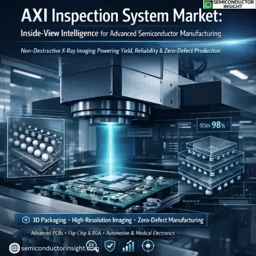
AXI Inspection System Market Growth Boosts Automated Quality Assurance, Expands Adoption, and Shapes Forecast Momentum
At the heart of modern semiconductor production lies an increasing need for visibility into densely packed circuitry, hidden layers, and minute structural features. Automated X-ray Inspection (AXI) systems have emerged as a cornerstone technology for non-destructive evaluation in electronics manufacturing. These systems allow manufacturers to look inside assemblies without disassembly, revealing defects that optical inspection cannot detect.
AXI inspection system market is not a niche add-on; it has become integral to achieving the yield, reliability, and throughput targets required by advanced nodes, 3D stacking, heterogeneous integration, and high-volume consumer electronics.
Defining the AXI Inspection System Market through Production Demands
AXI inspection systems are used to inspect a range of electronic assemblies from printed circuit boards (PCBs) to flip-chip packages, BGA (ball grid array) components, IC packaging, and through-silicon vias (TSVs) in advanced semiconductors. Traditional visual inspection and electrical tests often miss subsurface voids, solder voids, hidden cracks, or misplaced components. X-ray inspection fills this gap by providing volumetric imaging that captures both surface and internal features.
Industry adoption has grown as manufacturers pursue zero-defect production models, particularly in segments where failure rates as low as 0.1% can lead to costly recalls or functional failures.
Why Demand Is Rising: Shrinking Features and Rising Complexity
Two major structural forces drive demand for AXI inspection:
- Miniaturization of components: As interconnect pitches shrink below tens of microns and 3D packaging becomes common, physical access for probing and optical inspection becomes impossible.
- Complex integration strategies: Heterogeneous packages, multi-die arrangements, and mixed technologies introduce fault risks that can only be resolved by high-resolution internal imaging.
Statistical Signals Shaping the Market Landscape
Several statistical insights highlight how integral AXI systems have become:
- Nearly half of all advanced PCB assemblies undergo some form of X-ray inspection during manufacturing.
- The proportion of semiconductor packaging lines adopting 3D and multi-layer inspection platforms has increased by double-digit percentages year over year.
- A significant portion of automotive and medical electronics manufacturers now rely on 100% inspection coverage at critical stages to meet quality standards.
- Throughput expectations are climbing, with production lines requiring AXI cycle times that support daily multi-thousand PCB volumes.
Material and Technology Drivers in AXI System Development
From a semiconductor materials perspective, AXI systems must cope with a range of densities and compositions. High-density interconnects, metal-filled vias, and composite substrates challenge imaging systems to differentiate between materials with subtle density variations.
Recent technology advancements include:
- High-resolution detectors that capture finer detail without slowing throughput
- Multi-angle X-ray sources and computed tomography (CT) for comprehensive 3D reconstruction
- Advanced image processing algorithms that enhance defect recognition and classification
You can freely browse our most recent updated report to learn more about it before scrolling further:
https://semiconductorinsight.com/report/axi-inspection-system-market/
Integration with Smart Manufacturing and Data Platforms
While AXI systems generate high-fidelity images, their value is multiplied when connected to broader manufacturing execution systems (MES) and quality analytics platforms. Real-time defect data enables corrective action sooner, reduces rework cycles, and supports continuous improvement.
Manufacturers are increasingly linking AXI output to machine learning analytics to identify defect patterns, trace root causes, and refine process controls. This integration is part of a broader trend toward data-driven production quality management in semiconductor fabs and electronics assembly plants.
Applications across Industries and Critical Use Cases
AXI inspection is deployed across a range of sectors: From consumer electronics and telecommunication devices to automotive electronics, industrial controls, medical devices, and aerospace systems where reliability and safety requirements are stringent.
In automotive electronics alone, where components are expected to operate without failure under extreme vibration and temperature swings, X-ray inspection coverage is often mandated at multiple assembly stages. The proportion of automotive manufacturers integrating AXI in line has grown steadily as the number of semiconductor-reliant systems per vehicle continues to rise.
Market Expansion and Competitive Positioning
The competitive landscape in AXI systems includes established industrial imaging firms and specialized semiconductor equipment providers. Strategic differentiation often revolves around:
- Imaging resolution and defect recognition accuracy
- Throughput performance compatible with mass production
- Software ecosystem for integration with plant systems
- Service and calibration support network
Navigating Supply Chain Complexity and Adoption Barriers
Despite strong demand, some manufacturers face challenges in AXI implementation:
- Balancing inspection thoroughness with line speed
- Integrating diverse toolsets into existing production ecosystems
- Training and maintaining skilled operators for complex inspection scenarios
However, these challenges have encouraged investment in automated diagnosis, remote monitoring, and standardized inspection protocols, which are becoming common practice among global electronics producers.
Further, the evolution of the AXI inspection system market reflects a broader shift in semiconductor manufacturing from reactive quality control to proactive and predictive assurance. As complexity escalates and defect windows narrow, the value of inside-view inspection becomes not an option, but a fundamental requirement for reliable production.
What started as a specialty inspection capability has matured into a strategic pillar for manufacturing excellence, supporting everything from advanced logic packaging to high-reliability modules in critical systems.

Comments (0)