ASML Warns of Flat Growth While China’s SiCarrier and AMEC Push to Reshape Etching Equipment Landscape
In the high-stakes world of semiconductor manufacturing, etching equipment plays a pivotal role. As integrated circuits become more advanced and transistor nodes shrink to atomic scales, etching equipment has transitioned from a mere supporting tool to a central enabler of chip innovation. With the wafer used etching equipment market valued at US$ 12.34 billion in 2024 and projected to soar to US$ 23.89 billion by 2032, growing at a CAGR of 9.9%, it’s evident that this segment is undergoing a transformative evolution.
Access Your Free Sample Report- Wafer Used Etching Equipment Market
What Is Wafer Etching and Why It Matters
Wafer etching is a key process in the fabrication of semiconductor devices, used to selectively remove material from the surface of silicon wafers to create patterns for transistor structures. As chips become smaller and denser, precision etching becomes more difficult yet increasingly vital. Equipment must support sub-5nm and even atomic-layer nodes, with minimal material damage and impeccable uniformity.
There are two main etching types:
- Dry etching: Involves plasma or gases; preferred for finer patterns and lower contamination.
- Wet etching: Uses chemicals in liquid form; generally more cost-effective but less precise.
Modern fabs increasingly favor dry etching, especially reactive-ion etching (RIE) and atomic layer etching (ALE), as transistor sizes shrink below 7nm.
Market Size and Growth Drivers (2025–2032)
According to industry estimates, the wafer used etching equipment market is expected to expand from US$ 12.34 billion in 2024 to US$ 23.89 billion by 2032, growing at a compound annual growth rate of 9.9%.
Key Growth Factors:
- Increased demand for 5G and AI chips: These technologies require ultra-high-density semiconductor architectures.
- Miniaturization of devices: Nodes at 5nm and below require atomic-level etching precision.
- Booming consumer electronics market: Smartphones, smartwatches, and AR/VR devices all depend on high-performance chips.
- Government incentives and subsidies: Especially in China, India, and the U.S.
- Decarbonization goals: Demand for greener, energy-efficient etching equipment is growing.
Latest Industry Developments in 2024–2025
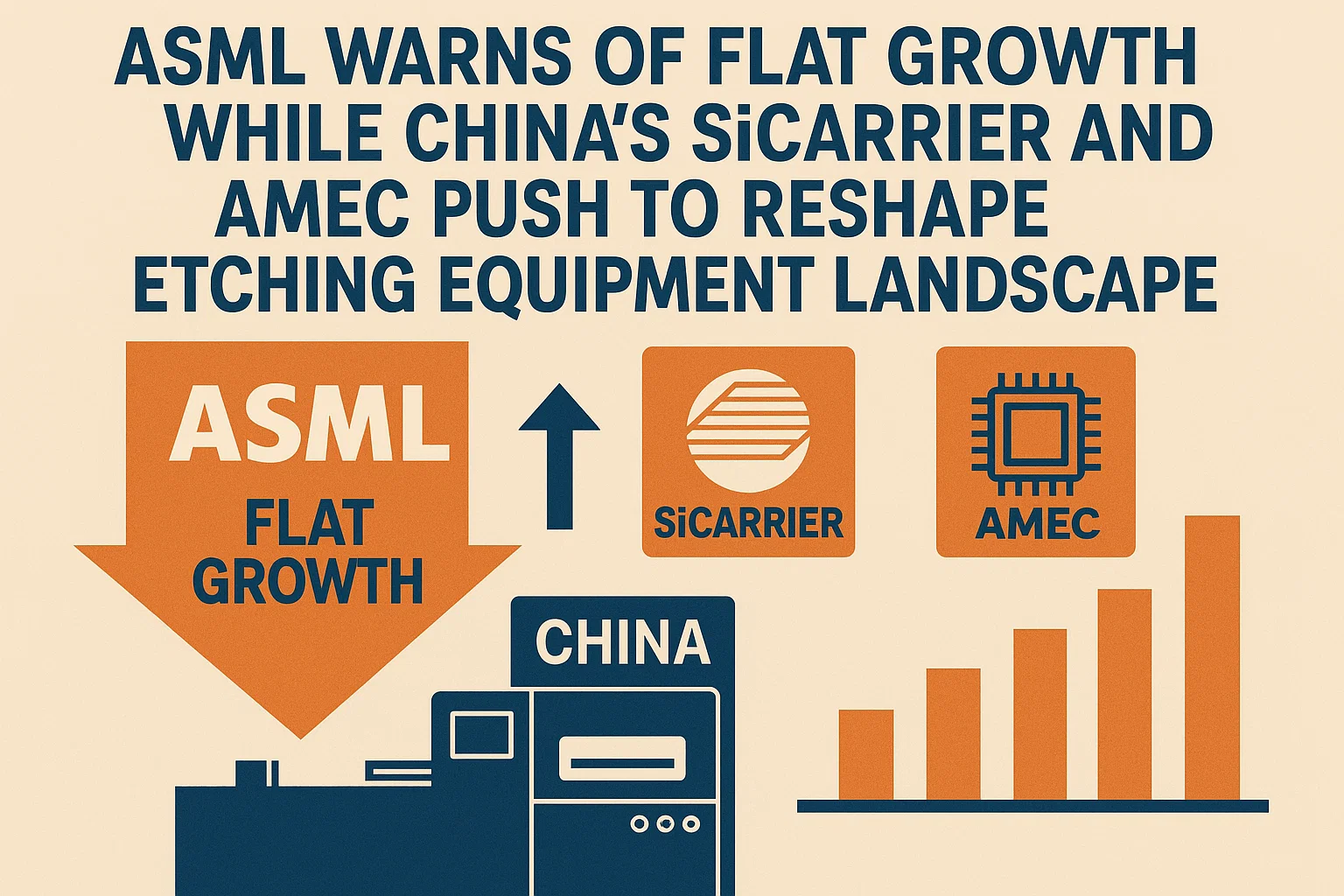
1. ASML Warns of Flat Growth Beyond 2025
ASML, a global titan in chip-making tools, especially extreme ultraviolet (EUV) lithography, has issued a cautious forecast for 2026, warning of flat growth. This stems from:
- Delayed customer investments due to geopolitical risks.
- Uncertainty from U.S.-China chip tensions.
- Saturation in advanced EUV tool demand in mature markets.
Although ASML doesn’t directly produce etching tools, its market signals reverberate throughout the semiconductor supply chain. When leading foundries pull back on lithography equipment, etching orders often follow.
“We cannot be overly optimistic in this environment,” stated ASML’s CEO in July 2024, citing U.S. export curbs and inflation concerns.
2. China’s Big Fund III: A Strategic Rethink
In a bold response to Western export bans, China’s $50 billion “Big Fund III” has been redirected toward:
- Etching, lithography, and EDA tool development.
- Reducing reliance on Western chip equipment giants.
- Supporting domestic firms like Naura, AMEC, and SiCarrier.
According to Reuters, the fund will no longer prioritize memory fabs or mobile processors, instead investing in the toolchain for producing them.
“This is not just about chips—it’s about the tools to make chips,” an insider told Reuters.
China’s increasing focus on etching technologies positions it as both a competitor and a growth engine for global equipment makers.
3. Rise of Local Champions: AMEC and Naura
Domestic Chinese firms like AMEC (Advanced Micro-Fabrication Equipment Inc.) and Naura Technology are seeing exponential growth:
- AMEC’s dry etching tools are now used at leading Chinese fabs.
- Naura posted over 60% YoY growth in etching equipment sales in 2024.
- Combined, they now command ~17% of the domestic etching market.
Although still trailing behind Tokyo Electron, Lam Research, and Applied Materials globally, these firms are closing the gap fast—fueled by subsidies, talent repatriation, and patent accumulation.
4. Huawei-backed SiCarrier’s $2.8 Billion Ambition
SiCarrier, a stealth-mode semiconductor tool firm backed by Huawei and local governments, has launched a $2.8 billion funding round. It aims to:
- Develop in-house plasma etchers and litho-inspection tools.
- Reduce reliance on Applied Materials and Lam Research tools.
- Present 30+ prototype tools by the end of 2025.
SiCarrier’s emergence could be a turning point in China’s semiconductor sovereignty strategy, especially if their tools pass quality validation at commercial fabs.
Download Sample Report PDF- Wafer Used Etching Equipment Market
Technology Trends Redefining Etching
1. Atomic Layer Etching (ALE)
ALE enables etching with atomic-scale precision, alternating between plasma and inert gas treatments to remove layers one atom at a time.
- Supports sub-3nm node fabrication.
- Enhances control over profile angles, selectivity, and uniformity.
- Reduces damage to delicate films in 3D NAND and logic devices.
Lam Research and Tokyo Electron are currently the leaders in commercial ALE systems, but Chinese and South Korean companies are rapidly developing their own alternatives.
2. AI-Powered Smart Etching Systems
Advanced etching tools are now embedded with AI/ML capabilities:
- Real-time process recipe optimization.
- Predictive maintenance to reduce tool downtime.
- Pattern recognition and etch-depth accuracy via computer vision.
This not only increases yield but shortens development cycles for new chip nodes.
3. Sustainable Etching Solutions
Environmental concerns are pushing fabs to adopt more eco-friendly tools:
- Plasma etchers now feature closed-loop gas recycling.
- PFC (perfluorocarbon) emissions are being cut by new abatement modules.
- Power consumption per wafer is a new KPI—especially in Taiwan, where energy rationing is a concern.
Green etching technologies are becoming a competitive differentiator in RFQ processes across Taiwan, Korea, and the EU.
Regional Focus: Asia-Pacific Leads, But with Nuance
Asia-Pacific dominates the global etching equipment market, comprising over 60% of global revenue. This is largely due to the presence of major fabs in:
- Taiwan (TSMC)
- South Korea (Samsung, SK Hynix)
- China (SMIC, CXMT, YMTC)
However, each region faces its own headwinds:
| Region | Advantage | Challenge |
| Taiwan | Home to the most advanced nodes (TSMC) | Power constraints, talent shortage |
| South Korea | Strong memory fabrication (Samsung, Hynix) | Export restrictions on Japan-origin tools |
| China | Largest market for growth, rapid local innovation | Blocked from ASML EUV, Lam/Applied exports |
Geopolitics and Export Restrictions: The Elephant in the Cleanroom
The semiconductor equipment industry is being fundamentally reshaped by geopolitics. The U.S., Japan, and the Netherlands have implemented coordinated export bans against China, targeting:
- EUV lithography systems (ASML)
- Advanced etching and deposition tools
- EDA software (Synopsys, Cadence)
As a result:
- Global firms must navigate dual compliance
- Chinese firms are fast-tracking domestic substitutes.
- Supply chains are being split into “friend-shored” vs. restricted markets.
This shift is not just a challenge—it’s a source of demand. As China builds more fabs with home-grown tools, both legacy and cutting-edge etchers are needed in bulk.
Competitive Landscape (2024 Snapshot)
Here’s how the competitive field looks today:
| Company | Market Share (Est.) | Strength |
| Lam Research | ~34% | Advanced ALE, 3D NAND expertise |
| Tokyo Electron | ~28% | Strong presence in Korea, DRAM market |
| Applied Materials | ~19% | Comprehensive portfolio |
| AMEC (China) | ~9% | Fast-growing, cost-effective |
| Naura (China) | ~8% | Focused on 28nm and above |
| Hitachi High-Tech | ~2% | Specialty dry etchers |
Forecast and Opportunities: 2025–2032
The etching equipment market is expected to enter a supercycle phase driven by:
- AI infrastructure buildouts: H100/G200 chip demand will fuel fab expansions.
- High-bandwidth memory (HBM) boom: Driven by GPUs and data centers.
- Automotive chips: Increasing complexity of EV and ADAS systems.
- Foundry diversification: India, Vietnam, and the Middle East entering the scene.
Strategic Opportunities:
- Equipment leasing models for mid-tier fabs.
- Retrofitting older tools for greener performance.
- Collaborative R&D hubs to reduce duplication and risk.
Click Here To Download Full Sample Report- Wafer Used Etching Equipment Market
A Market in Flux, But Full of Promise
As we look ahead, it’s clear the wafer used etching equipment industry is no longer a “back-end” afterthought—it’s the frontier of semiconductor innovation. Fueled by AI, geopolitics, green mandates, and fierce regional competition, the next decade promises radical change.
Global players must innovate faster while navigating export regulations, and rising stars—especially in China—must prove that domestic substitutes can match global performance.
For investors, engineers, policymakers, and technologists alike, this is a sector to watch closely. With a projected market value approaching US$ 24 billion by 2032, the cleanroom may just be the most important battleground of the decade.
Comments (0)