Wireless On-Wafer Temperature Measurement Systems Market Insights
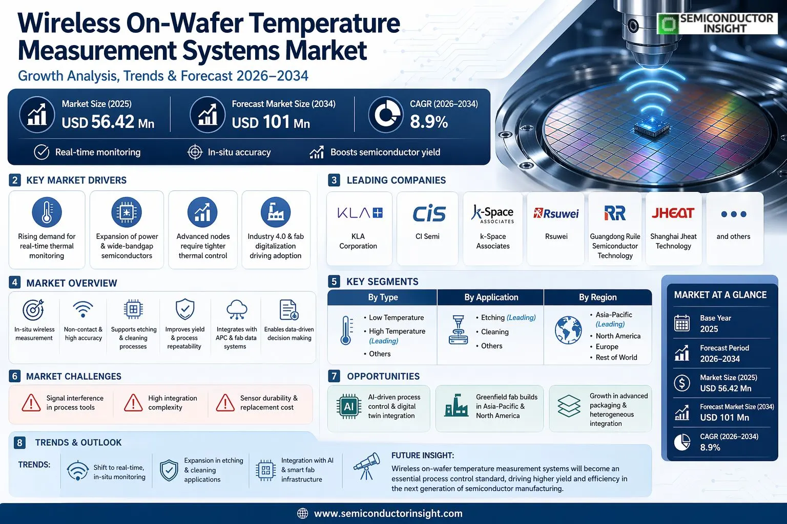
Global Wireless On-Wafer Temperature Measurement Systems market size was valued at USD 56.42 million in 2025. The market is projected to grow from USD 61.44 million in 2026 to USD 101 million by 2034, exhibiting a CAGR of 8.9% during the forecast period.
Wireless On-Wafer Temperature Measurement Systems embed a complete measurement system directly within the wafer, enabling accurate monitoring and recording of the impact of the semiconductor process environment on production wafers under real process conditions , all without the need for wired connections. These systems are designed to capture thermal data across critical semiconductor manufacturing processes, including etching and cleaning, spanning both low-temperature and high-temperature operational ranges.
The market is gaining significant traction driven by the rapid expansion of Global semiconductor industry, increasing demand for precision process control, and the growing complexity of advanced chip fabrication nodes. Furthermore, the push toward minimizing process variability and improving wafer yield in high-volume manufacturing environments has accelerated adoption of in-situ wireless measurement technologies. KLA Corporation, CI Semi, k-Space Associates, Rsuwei, Guangdong Ruile Semiconductor Technology, and Shanghai Jheat Technology are among the key players operating in the market, collectively accounting for a substantial share of global revenues in 2025.
MARKET DRIVERS
Rising Demand for Real-Time Thermal Monitoring in Advanced Semiconductor Fabrication
Wireless On-Wafer Temperature Measurement Systems Market is experiencing sustained growth driven by the increasing complexity of semiconductor manufacturing processes. As node sizes shrink below 5nm and 3nm geometries become more prevalent in high-volume manufacturing, precise thermal management during fabrication has become a critical quality parameter. Traditional wired temperature sensing solutions introduce mechanical constraints and contamination risks that are incompatible with cleanroom environments, making wireless alternatives increasingly essential for process engineers seeking non-contact, real-time thermal data across the wafer surface.
Expansion of Compound Semiconductor and Power Electronics Manufacturing
Growing investment in compound semiconductor materials such as gallium nitride (GaN), silicon carbide (SiC), and indium phosphide (InP) for power electronics, RF communications, and electric vehicle applications is a significant driver for Wireless On-Wafer Temperature Measurement Systems Market. These wide-bandgap materials are processed at elevated temperatures and exhibit strong sensitivity to thermal gradients during deposition and annealing. Wireless measurement systems capable of capturing spatial temperature distribution across compound semiconductor wafers enable manufacturers to optimize yield, reduce defect densities, and maintain tighter process control windows that conventional measurement methods cannot achieve.
➤ As semiconductor manufacturers accelerate transitions to advanced packaging formats including 2.5D and 3D IC integration, the need for wireless on-wafer thermal profiling tools capable of operating within complex multi-die environments is intensifying, positioning this technology as a foundational element of next-generation process control infrastructure.
The proliferation of AI and high-performance computing (HPC) chip manufacturing has placed unprecedented thermal management demands on front-end-of-line and back-end-of-line processes. Wireless on-wafer temperature measurement systems provide fabs and equipment vendors with actionable thermal maps that support rapid process qualification, chamber matching, and preventive maintenance scheduling , all of which are critical capabilities as leading-edge fabs scale to meet surging global chip demand.
MARKET CHALLENGES
Technical Complexity of Integrating Wireless Systems Within Controlled Cleanroom and Vacuum Environments
One of the most significant challenges facing Wireless On-Wafer Temperature Measurement Systems Market is the difficulty of deploying wireless communication hardware within semiconductor fabrication environments. Cleanrooms, plasma chambers, and chemical vapor deposition (CVD) reactors impose strict electromagnetic compatibility requirements and material restrictions that limit the types of wireless protocols and sensor materials that can be safely deployed. Engineers must navigate conflicts between RF signal integrity and process chamber shielding requirements, often requiring custom-engineered solutions that increase both development timelines and system costs.
Other Challenges
High System Cost and Integration Barriers
Wireless on-wafer temperature measurement systems represent a significant capital investment relative to conventional thermocouple or wired pyrometry solutions. The cost of developing wafer-compatible sensor arrays, wireless telemetry modules, and associated data acquisition software creates adoption barriers particularly for smaller fabs, research institutions, and emerging market participants operating under constrained capital expenditure budgets. Integration with existing fab automation and process control software platforms requires substantial customization, further elevating the total cost of ownership for early adopters in Wireless On-Wafer Temperature Measurement Systems Market.
Calibration, Standardization, and Data Validation Concerns
The absence of universally accepted calibration standards and measurement protocols for wireless on-wafer thermal sensing creates challenges in cross-platform data comparability and regulatory acceptance. Fabs adopting these systems must invest in rigorous internal validation processes to demonstrate measurement traceability and repeatability, which can slow procurement decisions and extend qualification cycles. The lack of industry-wide standardization remains an obstacle to broader commercialization across Wireless On-Wafer Temperature Measurement Systems Market.
MARKET RESTRAINTS
Regulatory and Safety Constraints Limiting Wireless RF Transmission in Semiconductor Process Equipment
Regulatory frameworks governing electromagnetic emissions in industrial and semiconductor manufacturing environments impose strict limits on the RF power levels and frequency bands permissible within process tools. These constraints directly affect the design feasibility of wireless on-wafer temperature measurement systems, particularly in plasma-based etch and deposition equipment where RF interference can compromise both measurement accuracy and process stability. Compliance with international electromagnetic compatibility (EMC) standards, including those defined by the IEC and SEMI equipment standards bodies, requires manufacturers to invest in extensive shielding and filtering designs that can reduce wireless signal range and increase system complexity within Wireless On-Wafer Temperature Measurement Systems Market.
Limited Sensor Durability and Lifespan Under Harsh Process Conditions
Wireless sensor nodes integrated onto wafers or process kits must withstand extreme thermal cycling, corrosive chemical exposure, and mechanical stress inherent in semiconductor manufacturing workflows. The durability of wireless sensor components , including antenna structures, power harvesting elements, and data transmission circuits , under repeated exposure to aggressive process chemistries such as fluorine-based plasmas or high-temperature oxidation environments remains a meaningful restraint on adoption within Wireless On-Wafer Temperature Measurement Systems Market. Short sensor service lifespans increase consumable costs and create operational disruptions that reduce the net economic value of wireless thermal monitoring solutions for high-volume manufacturing fabs.
MARKET OPPORTUNITIES
Integration of Wireless On-Wafer Temperature Measurement Systems with AI-Driven Process Control Platforms
The convergence of wireless thermal sensing technologies with artificial intelligence and machine learning-based process control platforms represents a substantial growth opportunity for Wireless On-Wafer Temperature Measurement Systems Market. Real-time spatial temperature data captured by wireless sensor arrays can serve as high-fidelity inputs to predictive process models, enabling adaptive control systems to automatically adjust recipe parameters in response to detected thermal non-uniformities. Semiconductor equipment OEMs and independent software vendors are actively developing integrated solutions that combine wireless on-wafer sensing with digital twin frameworks, creating new value propositions for leading-edge fabs focused on yield improvement and process stability.
Emerging Demand from Advanced Packaging and Heterogeneous Integration Applications
The rapid growth of advanced packaging technologies , including fan-out wafer-level packaging (FOWLP), chip-on-wafer-on-substrate (CoWoS), and hybrid bonding , is creating new application areas for wireless on-wafer temperature measurement within the back-end semiconductor supply chain. Thermal management during bonding, encapsulation, and underfill curing processes is critical to package reliability and long-term performance, and wireless measurement systems offer the spatial resolution and non-contact measurement capability required to characterize these thermally sensitive operations. As global investment in advanced packaging capacity accelerates in response to AI semiconductor demand, Wireless On-Wafer Temperature Measurement Systems Market is well positioned to benefit from expanded procurement by OSAT providers and integrated device manufacturers scaling heterogeneous integration workflows.
Geographic Expansion Driven by Regional Semiconductor Manufacturing Investments
Government-backed semiconductor manufacturing initiatives in the United States, European Union, Japan, South Korea, and India are driving substantial capacity additions across both logic and memory manufacturing segments. These greenfield and brownfield fab projects present a significant market opportunity for suppliers of wireless on-wafer temperature measurement systems, as new facilities are designed with modern process control architectures that can more readily accommodate wireless sensing infrastructure from initial tool qualification. Regional diversification of semiconductor production creates a geographically broader and more resilient customer base for Wireless On-Wafer Temperature Measurement Systems Market, reducing historical dependence on East Asian fab concentration and expanding total addressable market potential across multiple high-growth regions simultaneously.
Trends
Growing Semiconductor Process Complexity Driving Adoption of Wireless On-Wafer Temperature Measurement Systems
Wireless On-Wafer Temperature Measurement Systems Market is experiencing notable momentum as semiconductor manufacturers increasingly prioritize real-time, in-situ process monitoring. Unlike conventional wired measurement approaches, wireless on-wafer systems embed a complete measurement architecture directly into the wafer, enabling accurate temperature recording under actual process conditions without disrupting the manufacturing environment. This capability has become particularly critical as advanced node semiconductor fabrication demands tighter thermal control across etching, cleaning, and deposition processes. As chipmakers scale down to sub-5nm geometries, even marginal thermal deviations can compromise yield, making precise wafer-level temperature monitoring a strategic necessity rather than an optional tool.
Other Trends
Expansion Across Etching and Cleaning Applications
Among the primary application segments, etching and cleaning processes represent the most significant areas of adoption for Wireless On-Wafer Temperature Measurement Systems. Plasma etching, in particular, generates highly localized thermal gradients that are difficult to characterize with traditional off-wafer sensors. Wireless on-wafer systems provide manufacturers with granular thermal maps that allow process engineers to fine-tune parameters in real time. Similarly, in wafer cleaning operations, temperature uniformity is essential to ensure consistent chemical reaction rates across the wafer surface. The growing complexity of multi-step cleaning protocols in advanced logic and memory device manufacturing is further reinforcing demand for wireless measurement capabilities in this segment.
Segmentation Between Low Temperature and High Temperature Systems
Wireless On-Wafer Temperature Measurement Systems Market is segmented into low temperature and high temperature product categories, each serving distinct process environments. Low temperature systems are widely deployed in back-end-of-line processes and certain cleaning applications where thermal exposure is moderate. High temperature variants are engineered to withstand the demanding conditions found in epitaxial growth, rapid thermal processing, and high-power plasma etch chambers. As process diversity increases across leading-edge fabs, demand for both segments is rising in parallel, with manufacturers developing more robust wireless communication protocols and sensor materials to sustain accuracy across broader thermal ranges.
Regional Dynamics and Competitive Landscape Shaping Market Direction
From a regional perspective, Asia , particularly China, Japan, and South Korea , represents the most active market for Wireless On-Wafer Temperature Measurement Systems, driven by heavy investments in domestic semiconductor manufacturing capacity. North America remains a key innovation hub, with companies such as KLA Corporation and k-Space Associates playing prominent roles in advancing measurement system capabilities. Europe, led by Germany and other industrial semiconductor markets, is also registering steady uptake as fab operators upgrade legacy process control infrastructure. The competitive landscape includes both established metrology leaders and emerging regional players such as Guangdong Ruile Semiconductor Technology and Shanghai Jheat Technology, reflecting the market’s increasingly global and diversified supplier base. Ongoing investment in wireless sensor miniaturization, data transmission reliability, and compatibility with next-generation process tools continues to define differentiation strategies across Wireless On-Wafer Temperature Measurement Systems Market.
COMPETITIVE LANDSCAPE
Key Industry Players
Wireless On-Wafer Temperature Measurement Systems Market: Competitive Dynamics and Leading Innovators Shaping Global Semiconductor Metrology Space
Global Wireless On-Wafer Temperature Measurement Systems market is characterized by a moderately consolidated competitive landscape, with a handful of specialized technology companies commanding significant revenue share. KLA Corporation stands out as the dominant force in this space, leveraging its extensive semiconductor process control portfolio, global distribution network, and deep customer relationships with leading chip manufacturers. KLA’s advanced metrology and process monitoring capabilities position it as the preferred partner for high-volume fabs seeking reliable, real-time temperature data during critical wafer processing steps such as etching and cleaning. The top five global players collectively accounted for a substantial share of the market in 2025, underscoring the importance of technological differentiation, precision engineering, and established semiconductor industry partnerships in maintaining competitive advantage. As the market continues its projected growth trajectory from USD 56.42 million in 2025 toward USD 101 million by 2034 at a CAGR of 8.9%, competitive pressures are intensifying around product innovation, miniaturization, and wireless data transmission accuracy under demanding process environments.
Beyond the market leader, several niche yet strategically significant players are making meaningful inroads. CI Semi and k-Space Associates bring focused expertise in semiconductor measurement instrumentation, catering to fabs that require highly customized, application-specific solutions for both low-temperature and high-temperature process monitoring segments. Asian manufacturers, including Guangdong Ruile Semiconductor Technology and Shanghai Jheat Technology, are gaining competitive traction, particularly within China’s rapidly expanding domestic semiconductor ecosystem, driven by government-backed capacity expansion initiatives. Rsuwei also contributes to the competitive mix with cost-competitive offerings targeting mid-tier semiconductor manufacturers. The overall competitive environment is further shaped by ongoing R&D investment, strategic collaborations with equipment OEMs, and the growing need for wireless, non-invasive measurement systems that can operate seamlessly under real process conditions without wired connections , a core value proposition differentiating this market from conventional temperature measurement technologies.
List of Key Wireless On-Wafer Temperature Measurement Systems Companies Profiled
- KLA Corporation
- CI Semi
- k-Space Associates
- Rsuwei
- Guangdong Ruile Semiconductor Technology
- Shanghai Jheat Technology
Segment Analysis:
| Segment Category | Sub-Segments | Key Insights |
| By Type |
|
High Temperature systems represent the dominant segment within Wireless On-Wafer Temperature Measurement Systems Market, driven by the critical need to monitor and manage extreme thermal conditions prevalent in advanced semiconductor fabrication processes.
|
| By Application |
|
Etching is the leading application segment, commanding a prominent position in Wireless On-Wafer Temperature Measurement Systems Market owing to the highly temperature-sensitive nature of both dry and wet etching processes in semiconductor manufacturing.
|
| By End User |
|
Foundries represent the dominant end-user segment for Wireless On-Wafer Temperature Measurement Systems, reflecting the intense pressure on contract semiconductor manufacturers to optimize process stability, throughput, and yield across diverse customer technology nodes.
|
| By Technology |
|
RF-Based Wireless Transmission is the leading technology segment, underpinning the majority of deployed wireless on-wafer temperature measurement solutions due to its proven ability to reliably transmit sensor data through the electromagnetically complex environments found inside semiconductor process chambers.
|
| By Wafer Size |
|
300mm Wafers dominate the wafer size segment, as the mainstream standard for high-volume logic and memory semiconductor manufacturing, creating the largest addressable opportunity for wireless on-wafer temperature measurement systems globally.
|
Regional Analysis: Wireless On-Wafer Temperature Measurement Systems Market
Asia-Pacific hosts the highest density of active semiconductor fabrication plants globally. Continuous capacity expansions by leading foundries in Taiwan and South Korea, coupled with China’s aggressive domestic chip manufacturing push, are generating sustained and growing demand for wireless on-wafer temperature measurement systems as an integral component of yield optimization and process control strategies.
The transition toward advanced and extreme ultraviolet lithography process nodes across Asia-Pacific fabs demands unprecedented thermal uniformity and real-time wafer temperature monitoring. Wireless on-wafer temperature measurement systems are increasingly regarded as critical enablers of defect reduction and process repeatability, particularly as thermal budgets become increasingly constrained at cutting-edge node geometries.
Strategic national programs across Japan, South Korea, China, and India are directing substantial public investment into domestic semiconductor ecosystems. These policy frameworks incentivize the procurement of advanced process monitoring equipment, including wireless on-wafer temperature measurement systems, supporting accelerated technology adoption and localization of high-precision measurement capabilities within regional supply chains.
Asia-Pacific benefits from a mature and deeply integrated semiconductor equipment supplier ecosystem. Local and international metrology vendors are actively collaborating with regional foundries to co-develop and validate wireless on-wafer temperature measurement systems tailored to specific process chemistries and chamber configurations, fostering rapid innovation cycles and faster commercialization of next-generation thermal sensing platforms.
North America
North America represents a strategically significant market for wireless on-wafer temperature measurement systems, underpinned by a well-established base of semiconductor research institutions, leading equipment manufacturers, and a resurgent domestic chip fabrication landscape. The United States, in particular, has witnessed a pronounced policy-driven revival of domestic semiconductor manufacturing, with major foundry investments underway across multiple states. This renaissance is creating fresh demand for advanced process metrology tools, including wireless on-wafer temperature measurement systems, as new and retrofitted fabs seek best-in-class thermal monitoring capabilities. The region’s concentration of fabless chip designers, integrated device manufacturers, and materials companies fosters a rich innovation environment where novel wireless sensing technologies are validated and commercialized. Additionally, North America’s strong intellectual property framework and proximity to leading research universities and national laboratories ensure a continuous pipeline of fundamental and applied research supporting the evolution of on-wafer temperature measurement methodologies through the forecast period.
Europe
Europe occupies a meaningful and evolving position in Wireless On-Wafer Temperature Measurement Systems Market, characterized by its strengths in precision instrumentation, automotive semiconductor applications, and power electronics manufacturing. Countries such as Germany, the Netherlands, and France host globally competitive semiconductor equipment vendors and specialized chip manufacturers whose processes demand stringent thermal control. The European Chips Act and related industrial policy initiatives are stimulating investments in domestic semiconductor production capacity, broadening the installed base of advanced fabrication tools that incorporate or require wireless on-wafer temperature measurement systems. Europe’s automotive and industrial sectors, which are among the largest consumers of power semiconductors and compound semiconductor devices, impose particularly demanding thermal management and measurement requirements. The region’s emphasis on sustainability and energy-efficient manufacturing processes further reinforces the relevance of precise, real-time wireless thermal monitoring as a means of minimizing energy waste and improving overall fab operational efficiency.
South America
South America currently represents an emerging and nascent segment of Global wireless on-wafer temperature measurement systems market. The region lacks the dense semiconductor manufacturing infrastructure present in Asia-Pacific and North America; however, growing electronics assembly activity in Brazil and increasing technology transfer initiatives are gradually building awareness and foundational demand for advanced process measurement tools. Academic and research institutions in Brazil and Argentina are engaging with semiconductor metrology concepts as part of broader scientific and industrial modernization programs. While near-term adoption of wireless on-wafer temperature measurement systems in South America is expected to remain limited relative to other regions, longer-term development of the region’s electronics and technology manufacturing sector could open incremental opportunities, particularly as global supply chain diversification strategies encourage broader geographic distribution of semiconductor-related investments and capabilities.
Middle East & Africa
The Middle East and Africa region is at an early stage of engagement with Wireless On-Wafer Temperature Measurement Systems Market. The Middle East, particularly the United Arab Emirates and Saudi Arabia, is investing in technology and innovation ecosystems as part of ambitious economic diversification agendas, which include nascent interest in semiconductor research and advanced electronics manufacturing. While large-scale wafer fabrication infrastructure remains limited across the region, collaborative academic programs and partnerships with global semiconductor companies are planting the seeds for longer-term market development. Africa’s engagement with this market remains largely indirect, mediated through electronics consumption rather than production. Nevertheless, the region’s growing emphasis on digital infrastructure and technology-driven economic growth positions it as a potential long-term participant in the broader semiconductor value chain, which could gradually stimulate demand for advanced measurement systems including wireless on-wafer temperature measurement platforms over the extended forecast horizon.
Report Scope
This market research report provides a comprehensive analysis of Wireless On-Wafer Temperature Measurement Systems Market, covering the forecast period 2026–2034. It offers detailed insights into market dynamics, technological advancements, competitive landscape, and key trends shaping the industry.
Key focus areas of the report include:
- Market Overview: The report begins with an overview outlining its current market scenario, key growth indicators, and industry transformation drivers. It discusses macroeconomic factors, demand–supply balance, regulatory landscape, and the strategic role of semiconductors in powering advancements across industries such as automotive, telecommunications, consumer electronics, and industrial automation.
- Market Size & Forecast: Historical data and future projections for revenue, unit shipments, and market value across major regions and segments.
- Segmentation Analysis: Detailed breakdown by product type, technology, application, and end-user industry to identify high-growth segments and investment opportunities.
- Regional Insights: Insights into market performance across North America, Europe, Asia-Pacific, Latin America, and the Middle East & Africa, including country-level analysis where relevant.
- Competitive Landscape: Profiles of leading market participants, including their product offerings, R&D focus, manufacturing capacity, pricing strategies, and recent developments such as mergers, acquisitions, and partnerships.
- Technology Trends & Innovation: Assessment of emerging technologies, integration of AI/IoT, semiconductor design trends, fabrication techniques, and evolving industry standards.
- Market Drivers & Restraints: Evaluation of factors driving market growth along with challenges, supply chain constraints, regulatory issues, and market-entry barriers.
- Stakeholder Insights: Insights for component suppliers, OEMs, system integrators, investors, and policymakers regarding the evolving ecosystem and strategic opportunities.
Primary and secondary research methods are employed, including interviews with industry experts, data from verified sources, and real-time market intelligence to ensure the accuracy and reliability of the insights presented.
FREQUENTLY ASKED QUESTIONS:
What is the current market size of Wireless On-Wafer Temperature Measurement Systems Market?
-> Global Wireless On-Wafer Temperature Measurement Systems Market was valued at USD 56.42 million in 2025 and is expected to reach USD 101 million by 2034, growing at a CAGR of 8.9% during the forecast period.
Which key companies operate in Wireless On-Wafer Temperature Measurement Systems Market?
-> Key players include KLA Corporation, CI Semi, k-Space Associates, Rsuwei, Guangdong Ruile Semiconductor Technology, and Shanghai Jheat Technology, among others.
What are the key growth drivers?
-> Key growth drivers include rising demand for real-time process monitoring in semiconductor fabrication, increasing adoption of wireless measurement technologies, expansion of semiconductor manufacturing capacity globally, and the need for accurate temperature measurement under real process conditions without wired connections.
Which region dominates the market?
-> Asia is a leading region in Wireless On-Wafer Temperature Measurement Systems Market, driven by strong semiconductor manufacturing activity in China, Japan, South Korea, and Southeast Asia, while North America remains a significant market with major players and technological innovation.
What are the emerging trends?
-> Emerging trends include integration of wireless sensing technologies in wafer-level process monitoring, development of low and high temperature measurement segment solutions, growing adoption in etching and cleaning applications, and increasing R&D investments by key manufacturers to enhance system accuracy and reliability.

Get Sample Report PDF for Exclusive Insights
Report Sample Includes
- Table of Contents
- List of Tables & Figures
- Charts, Research Methodology, and more...


