Wafer Thinning Grinding Wheel Market Insights
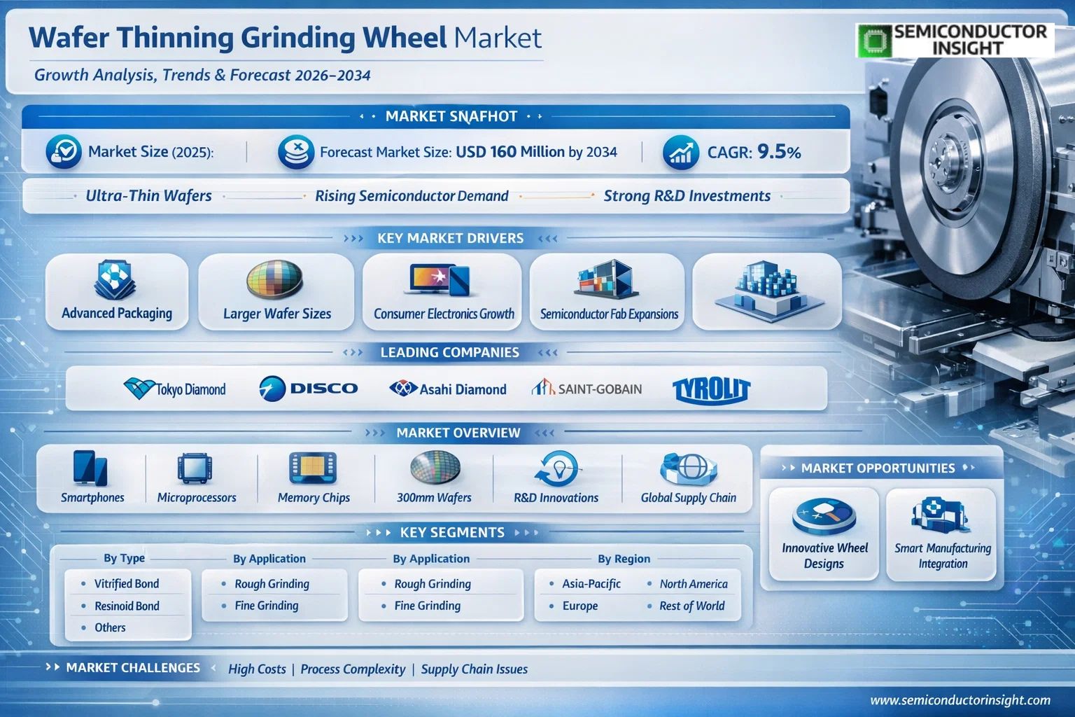
Wafer Thinning Grinding Wheel market size was valued at USD 85.1 million in 2025. The market is projected to grow from USD 93.1 million in 2026 to USD 160 million by 2034, exhibiting a CAGR of 9.5% during the forecast period.
A Wafer Thinning Grinding Wheel is a specialized abrasive tool used in semiconductor manufacturing to reduce the thickness of silicon wafers while maintaining their structural integrity and surface quality. This process, known as wafer thinning, is critical for producing ultra-thin wafers used in advanced electronic devices like smartphones, microprocessors, and memory chips. The grinding wheel typically features a diamond abrasive layer, ensuring precision, minimal damage, and high efficiency. Its design and material composition are optimized to handle the delicate nature of wafers while achieving the required thickness and flatness.
The market is experiencing robust growth due to several factors, including the relentless demand for smaller, more powerful consumer electronics and the expansion of advanced packaging technologies like Fan-Out Wafer-Level Packaging (FOWLP). Furthermore, the transition to larger wafer diameters such as 300mm necessitates highly precise thinning equipment. Initiatives by key players are also expected to fuel market growth; for instance, leading manufacturers continuously invest in R&D to develop wheels with superior bond systems for reduced chipping and improved surface finish. Tokyo Diamond Tools Mfg. Co., Ltd., Disco Corporation, Asahi Diamond Industrial Co., Ltd., Saint-Gobain S.A., and Noritake Co., Limited are some of the key players that operate in this highly specialized market with a wide range of portfolios.
MARKET DRIVERS
Demand from Advanced Semiconductor Packaging
The relentless push for more powerful and compact consumer electronics is a primary force propelling the wafer thinning grinding wheel market. Advanced packaging solutions like Fan-Out Wafer-Level Packaging (FO-WLP) and 3D IC stacking require ultra-thin wafers to achieve the necessary form factors and performance. This critical manufacturing step depends on high-precision grinding wheels to thin silicon wafers to specifications often below 100 micrometers without inducing subsurface damage. The demand for these specialized tools is directly correlated with the production volumes of cutting-edge chips for smartphones, high-performance computing, and artificial intelligence accelerators.
Adoption of Larger Wafer Diameters
The industry’s transition from 200mm to 300mm wafers and the ongoing development of 450mm platforms create a sustained need for advanced grinding solutions. Larger wafers offer greater economies of scale but present significant technical challenges during the thinning process, requiring grinding wheels with exceptional uniformity, stability, and durability to handle the increased surface area and mechanical stresses. This transition necessitates continuous R&D investment from wheel manufacturers, driving product innovation and market growth.
➤ A broader industry trend toward Total Thickness Variation (TTV) control below 2 micrometers is forcing grinding wheel technology to evolve, making precision a key purchasing criterion.
Furthermore, the expansion of the semiconductor ecosystem into new geographical regions and the establishment of new fabrication facilities globally are creating additional, sustained demand for consumables like wafer thinning grinding wheels, supporting long-term market expansion.
MARKET CHALLENGES
Technical Complexity and Process Control
A central challenge in the wafer thinning grinding wheel market is the extreme technical precision required. The process must achieve nanoscale surface finish and strict Total Thickness Variation (TTV) targets while completely avoiding micro-cracks or chipping that can ruin expensive wafers. This demands not only advanced wheel materials like fine-grit diamond or CBN but also perfect harmony with the grinding machine, coolants, and process parameters. Any inconsistency can lead to catastrophic yield loss, placing immense pressure on wheel consistency and performance validation.
Other Challenges
High Cost of Ownership and Qualification
Premium grinding wheels, especially those designed for the final “touch” finish, carry a significant cost. The lengthy and rigorous qualification process required by semiconductor manufacturers to validate a new wheel for high-volume production represents a major barrier to entry for new suppliers and slows adoption cycles for new technologies.
Supply Chain for Critical Raw Materials
The production of high-performance grinding wheels relies on specialized super-abrasive materials and engineered bonds. Fluctuations in the availability or price of high-quality synthetic diamonds or specific metal powders can disrupt manufacturing and impact the stability of the wafer thinning grinding wheel market.
MARKET RESTRAINTS
Emergence of Alternative Thinning Technologies
The growth potential of the traditional grinding wheel segment faces a degree of restraint from the development of competitive wafer thinning methods. Technologies like chemical-mechanical polishing (CMP) and various plasma-based etching techniques are being refined for specific applications, particularly where ultra-low damage or extreme thinness is required. While mechanical grinding remains the workhorse for bulk material removal, the encroachment of these alternatives for final finishing steps could limit the addressable market for certain high-value grinding wheel products.
Cyclical Nature of Semiconductor Capital Expenditure
The wafer thinning grinding wheel market is inherently tied to the capital investment cycles of Global semiconductor industry. During periods of reduced fab spending or inventory correction, manufacturers delay tool purchases and extend the lifecycle of existing consumables. This cyclicality can lead to volatility in demand, making long-term production planning and inventory management a complex challenge for suppliers in this space.
MARKET OPPORTUNITIES
Innovation in Wheel Composition and Design
Significant opportunity exists for companies that can innovate in wheel material science and architecture. Developing next-generation bonds that offer longer life, more consistent wear, and embedded lubricity can dramatically reduce the cost-of-ownership for chipmakers. Furthermore, wheels engineered for new substrate materials like silicon carbide (SiC) and gallium nitride (GaN) for power electronics present a high-growth niche, as these harder, more brittle materials require specialized grinding solutions distinct from those used for traditional silicon.
Integration with Smart Manufacturing and Industry 4.0
The integration of sensor technology and data analytics into the wafer thinning process creates a substantial opportunity. “Smart” grinding wheels equipped with sensors to monitor wear, vibration, and temperature in real-time can enable predictive maintenance, optimize grinding parameters on-the-fly, and provide traceability data. This alignment with Industry 4.0 trends offers a path to premium, value-added products that improve overall equipment effectiveness (OEE) for semiconductor manufacturers.
The sustained global investment in domestic semiconductor manufacturing capabilities, driven by geopolitical and supply chain resilience initiatives, is building a strong foundation for future demand. Each new fab represents a long-term stream of consumable purchases, ensuring a robust and growing addressable market for advanced wafer thinning grinding wheel suppliers who can meet the technical and logistical demands of these facilities.
Wafer Thinning Grinding Wheel Market Trends
Expansion in Application-Specific Grinding Wheel Design
A primary trend in the Wafer Thinning Grinding Wheel market is the shift towards application-specific designs, driven by the increasing complexity of semiconductor devices. Manufacturers are developing wheels tailored for distinct processes such as rough grinding and fine grinding, each requiring different abrasive grit sizes, bond materials, and wheel structures. The vitrified bond segment is seeing particular focus for its balance of rigidity and friability, essential for achieving superior surface finishes and controlling wafer stress. This trend is a direct response to the industry’s need for higher yield rates and the handling of advanced materials like compound semiconductors, which demand specialized grinding solutions to prevent micro-cracks and delamination.
Other Trends
Material Innovation and Diamond Abrasive Evolution
Continuous material science advancements represent a key trend. Innovations in diamond abrasive technology, including the development of mono-crystalline and nano-crystalline diamond particles, are enhancing wheel performance. These superior abrasives offer increased durability and more consistent cutting edges, which extend wheel life and improve the uniformity of the wafer thinning process. This evolution is critical for reducing consumable costs and improving throughput in high-volume semiconductor fabs, directly impacting the operational efficiency of the Wafer Thinning Grinding Wheel market.
Intensifying Competition and Strategic Focus Among Key Players
The competitive landscape is marked by intensified efforts from established leaders like Tokyo Diamond, Disco, and Asahi Diamond to consolidate market share through product development and strategic initiatives. A notable trend is the expansion of R&D focused on improving bond systems and wheel geometry to reduce chipping and improve flatness tolerances. Concurrently, companies are strengthening their supply chains and regional manufacturing presence to better serve key markets in Asia, particularly China and South Korea, which are hubs for semiconductor fabrication.
Regional Demand Shifts and Supply Chain Realignment
Geographic demand patterns are evolving, influencing market strategies. While established regions remain significant, growth is increasingly concentrated in Asia-Pacific, driven by major semiconductor manufacturing expansions. This shift is prompting suppliers in the Wafer Thinning Grinding Wheel market to realign production and distribution networks to ensure just-in-time delivery and technical support. The trend underscores the importance of regional adaptability and closeness to major wafer fabrication plants as a competitive advantage, alongside maintaining the high precision and reliability required for advanced node semiconductor production.
COMPETITIVE LANDSCAPE
Key Industry Players
A Market Characterized by Japanese Specialization, Global Materials Giants, and Emerging Asian Suppliers
Wafer Thinning Grinding Wheel market is characterized by a high degree of concentration around specialized manufacturers with deep expertise in super-abrasives and precision machining for the semiconductor industry. The competitive landscape is led by established Japanese players such as Disco, Tokyo Diamond, and Asahi Diamond, who collectively hold a significant revenue share. These leaders dominate due to their technological edge in diamond abrasive formulation and wheel design, critical for achieving the sub-micron precision, low subsurface damage, and high yield rates demanded in advanced nodes for logic and memory devices. Competition is intense, driven by R&D investments for finer, more durable vitrified and resinoid bond systems to handle increasingly thin and large-diameter wafers.
Beyond the Japanese leaders, the market features significant participation from major European abrasives conglomerates and emerging regional suppliers. Companies like Saint-Gobain and the Tyrolit Group leverage their global materials science expertise to provide competitive solutions. Meanwhile, other established Asian players such as Kinik, EHWA Diamond, and Shinhan Diamond hold strong positions, often serving domestic and regional foundry and packaging facilities. The market also sees growing activity from Chinese manufacturers like Qingdao Gaoce Technology, focusing on cost-competitive offerings for the expansive local semiconductor supply chain. Intense focus on quality, consistency, and technical support is essential for competing in this advanced materials segment.
List of Key Wafer Thinning Grinding Wheel Companies Profiled
- Tokyo Diamond
- Disco Corporation
- Asahi Diamond Industrial Co., Ltd.
- Saint-Gobain
- Tyrolit Group
- Noritake Co., Limited
- Kinik Company
- EHWA Diamond Industrial Co., Ltd.
- Shinhan Diamond Industrial Co., Ltd.
- Qingdao Gaoce Technology Co., Ltd.
- Kure Grinding Wheel Co., Ltd.
- Zhengzhou Research Institute For Abrasives & Grinding
- Suzhou Sail Science & Technology
Segment Analysis:
| Segment Category | Sub-Segments | Key Insights |
| By Type |
|
Vitrified Bond is the leading segment due to its exceptional performance in high-precision semiconductor manufacturing. The growth is driven by the wheel’s superior thermal and chemical stability, which minimizes wafer damage during aggressive thinning processes. Furthermore, its porous structure offers excellent chip clearance, reducing heat buildup and improving surface finish, which is critical for advanced node technologies. Manufacturers favor this bond type for its balance of hardness and ability to be easily dressed, ensuring consistent performance over the wheel’s lifecycle in demanding fabrication environments. |
| By Application |
|
Fine Grinding represents the dominant and most technologically intensive application segment. This process is crucial for achieving the ultra-thin wafer profiles required in modern 3D IC stacking and advanced memory packages. The segment’s leadership is anchored in the relentless industry push for miniaturization, which demands exceptional surface integrity and sub-micron thickness control. Innovation here focuses on minimizing sub-surface damage and stress to preserve wafer strength, directly influencing final device yield and performance in end-products like high-performance computing chips and mobile processors. |
| By End User |
|
Foundries are the leading end-user segment, driving significant demand for high-performance grinding wheels. Their pivotal role stems from serving a vast array of fabless semiconductor companies, requiring them to maintain cutting-edge thinning capabilities across diverse process nodes. This segment prioritizes wheels that offer exceptional consistency and longevity to maximize throughput and cost-efficiency in high-volume production. The competitive landscape among foundries compels continuous adoption of advanced grinding solutions to attract design wins for next-generation applications, including AI accelerators and 5G chipsets. |
| By Bonding Technology |
|
Hybrid Bond Systems are emerging as a key innovative segment, gaining traction for specialized applications. These systems combine materials like resin and metal to create wheels with tailored properties, such as enhanced toughness for difficult-to-grind materials like silicon carbide or gallium nitride wafers. The development focus is on achieving a superior balance between abrasive retention and elastic modulus to control grinding forces more precisely. This technology is particularly relevant for the nascent but growing market in power semiconductor and RF device manufacturing, where material properties differ significantly from traditional silicon. |
| By Wafer Size |
|
300mm is the unequivocal leading segment, representing the mainstream standard for high-volume semiconductor production. The demand is directly tied to the superior economies of scale and manufacturing efficiency this wafer size offers for leading-edge logic and memory chips. Grinding wheels for 300mm wafers necessitate extreme dimensional stability and uniformity to manage the larger surface area and prevent stress-induced warping or breakage. The technical complexity and capital intensity of 300mm fabrication lines create a high-value, captive market for premium grinding wheels, with stringent requirements driven by the need for flawless yield management. |
Regional Analysis: Asia-Pacific Wafer Thinning Grinding Wheel Market
East Asia
Japan remains a critical hub for high-end, specialized grinding wheel technology, supplying ultra-precision tools for applications like silicon carbide and gallium nitride wafers used in power electronics and RF devices. Its market is characterized by deep collaborations between toolmakers and equipment OEMs to deliver integrated solutions.
The entire value chain for wafer thinning grinding wheels, from advanced abrasive grain production to final wheel fabrication and application engineering, is densely concentrated in East Asia. This localization reduces lead times and fosters rapid iteration, directly serving the needs of the world’s largest semiconductor fabs.
South Korea and Taiwan are home to the world’s leading memory makers and pure-play foundries. Their massive, ongoing capital expenditures for cutting-edge nodes directly fuel demand for grinding wheels with superior dimensional accuracy and sub-surface damage control to enable subsequent ultra-thinning processes.
China’s rapidly expanding domestic semiconductor industry, bolstered by significant national policy support, represents the fastest-growing demand segment for wafer thinning grinding wheels within East Asia. This growth spans both legacy node capacity build-outs and ambitious forays into advanced packaging technologies.
Southeast Asia & Oceania
The wafer thinning grinding wheel market in Southeast Asia and Oceania is primarily driven by the growing semiconductor backend operations, especially in Singapore, Malaysia, and the Philippines. Major OSATs and IDMs have established significant packaging and test facilities in this region, creating consistent demand for reliable wafer thinning solutions. The market trend here favors a mix of advanced and mature grinding wheel technologies to support a diverse product portfolio, from high-volume consumer chips to specialized automotive and industrial semiconductors. The investment climate and government incentives for high-tech manufacturing continue to attract capacity expansions, which in turn supports steady, growth-oriented demand for these consumable tools.
North America
North America’s wafer thinning grinding wheel market is defined by high-value R&D and pilot-line applications, supporting leading-edge logic and compound semiconductor development. Demand is concentrated around major IDMs, fabless design houses, and research consortia focusing on technologies like heterogeneous integration and chiplets. The regional market prioritizes grinding wheels that enable R&D for next-generation architectures rather than high-volume production. Collaborations between wheel suppliers, equipment manufacturers, and end-users are exceptionally close, focusing on solving specific technical challenges related to new materials and ultra-thin die requirements, making it an innovation-led segment of Global market.
Europe
The European wafer thinning grinding wheel market is characterized by specialized, high-precision applications, particularly in the automotive, industrial, and research sectors. Key demand stems from manufacturers of power semiconductors, MEMS sensors, and photonics devices, which require meticulous thinning processes. The regional focus is on grinding wheels that deliver exceptional consistency and low damage for niche, high-reliability applications. Strong collaboration exists between European toolmakers, research institutes, and equipment suppliers to develop tailored solutions for compound semiconductors like SiC and GaN, positioning this market as a leader in high-value, application-specific grinding technologies.
Rest of Asia-Pacific (South & Central Asia)
The wafer thinning grinding wheel market in the broader Rest of Asia-Pacific region, including South and Central Asia, is in a nascent but developing stage. Initial demand is emerging primarily from electronics assembly and lower-end semiconductor packaging activities. As countries seek to move up the value chain, there is potential for future growth linked to government initiatives aimed at developing domestic electronics manufacturing ecosystems. Currently, the market is served by imports of standardized grinding wheel products, with the long-term trajectory dependent on successful foreign direct investment and the establishment of more advanced semiconductor fabrication or packaging facilities within these developing economies.
Report Scope
This market research report provides a comprehensive analysis of the Wafer Thinning Grinding Wheel Market , covering the forecast period 2026–2034. It offers detailed insights into market dynamics, technological advancements, competitive landscape, and key trends shaping the industry.
Key focus areas of the report include:
- Market Overview: The report begins with an overview outlining the current market scenario, key growth indicators, and industry transformation drivers. It discusses macroeconomic factors, demand–supply balance, regulatory landscape, and the strategic role of semiconductor manufacturing in powering advancements across industries such as consumer electronics, automotive, telecommunications, and industrial automation.
- Market Size & Forecast: Historical data and future projections for revenue, unit shipments (K Units), and market value across major regions and segments.
- Segmentation Analysis: Detailed breakdown by product type (Vitrified Bond, Resinoid Bond, Others), application (Rough Grinding, Fine Grinding), and end-user industry to identify high-growth segments and investment opportunities.
- Regional Insights: Insights into market performance across North America, Europe, Asia, South America, and the Middle East & Africa, including country-level analysis for key nations like the U.S., China, Japan, and Germany.
- Competitive Landscape: Profiles of leading market participants, including their product offerings, manufacturing capacity, sales and revenue market share, pricing strategies, and recent developments such as mergers, acquisitions, and partnerships.
- Technology Trends & Innovation: Assessment of emerging technologies, fabrication techniques, advancements in diamond abrasive tool design, and evolving industry standards for wafer thinning and surface quality.
- Market Drivers & Restraints: Evaluation of factors driving market growth along with challenges, supply chain constraints, regulatory issues, and potential risks faced by manufacturers.
- Stakeholder Insights: Strategic insights for component suppliers, OEMs, system integrators, investors, and policymakers regarding the evolving semiconductor ecosystem and business opportunities.
Primary and secondary research methods are employed, including surveys of manufacturers, suppliers, and industry experts, analysis of sales and revenue data from verified sources, and real-time market intelligence to ensure the accuracy and reliability of the insights presented.
FREQUENTLY ASKED QUESTIONS:
What is the current market size of Wafer Thinning Grinding Wheel Market?
-> Wafer Thinning Grinding Wheel market was valued at USD 85.1 million in 2025 and is projected to reach USD 160 million by 2034, growing at a CAGR of 9.5% during the forecast period.
Which key companies operate in Wafer Thinning Grinding Wheel Market?
-> Key players include Tokyo Diamond, Disco, Asahi Diamond, Saint-Gobain, Tyrolit Group, Noritake, Kinik, EHWA Diamond, Shinhan Diamond, and Qingdao Gaoce Technology, among others. In 2025, Global top five players held a significant share of the market revenue.
What are the key growth drivers?
-> Key growth drivers include the rising demand for ultra-thin wafers in advanced electronic devices (smartphones, microprocessors, memory chips), investments in semiconductor manufacturing capacity, and the need for precision tools that ensure structural integrity and surface quality during wafer thinning.
What are the primary market segments by type?
-> The market is segmented by type into Vitrified Bond, Resinoid Bond, and Others. The Vitrified Bond segment is a key focus area with significant projected growth.
Which region is a major market for Wafer Thinning Grinding Wheel?
-> Asia is a major and fast-growing market, with significant manufacturing activities and demand in countries like China, Japan, and South Korea. The U.S. market is also a substantial contributor to Global market size.

Get Sample Report PDF for Exclusive Insights
Report Sample Includes
- Table of Contents
- List of Tables & Figures
- Charts, Research Methodology, and more...