Wafer Thin Film Inspection Systems Market Insights
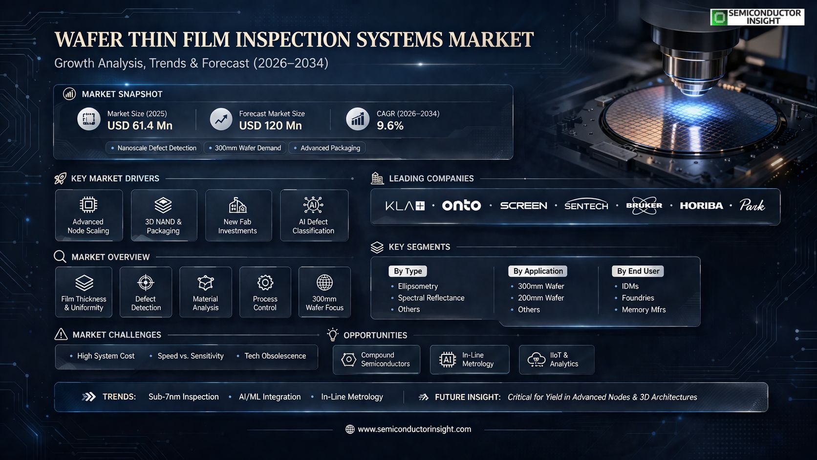
Global wafer thin film inspection systems market size was valued at USD 61.4 million in 2025. The market is projected to grow from USD 67.3 million in 2026 to USD 120 million by 2034, exhibiting a CAGR of 9.6% during the forecast period.
Wafer thin film inspection systems are advanced analytical tools used in semiconductor manufacturing to detect, measure, and analyze defects, uniformity, and properties of thin films deposited on semiconductor wafers. These systems ensure that the thin films meet strict quality and performance standards required for high-precision electronic devices. The primary technologies include ellipsometry, spectral reflectance, and other optical metrology techniques.
The market is experiencing robust growth due to several factors, including the relentless demand for more powerful and miniaturized semiconductors, which necessitates increasingly stringent process control. Furthermore, the expansion of 300mm wafer production capacity globally and the rise of advanced packaging technologies are significant drivers. Initiatives by key players are also propelling innovation; for instance, companies like KLA Instruments, Onto Innovation, and SCREEN Semiconductor Solutions continuously enhance their inspection platforms with higher throughput and sensitivity for next-generation nodes.
MARKET DRIVERS
Advancements in Semiconductor Manufacturing Nodes
The relentless drive toward smaller semiconductor manufacturing nodes below 7nm and 5nm is a primary market driver. As features shrink, detecting nanoscale defects on wafer thin films becomes exponentially more critical. This has led to increased adoption of advanced Wafer Thin Film Inspection Systems for metrology and defect review.
Rising Complexity of 3D NAND and Advanced Packaging
The growth of 3D NAND flash memory and heterogeneous integration using advanced packaging technologies like chiplets has amplified the demand for sophisticated inspection capabilities. These complex structures with multiple thin film layers require inspection systems with enhanced sensitivity and 3D analysis, directly boosting the Wafer Thin Film Inspection Systems Market.
➤ Investment in new fabrication facilities (fabs) dedicated to cutting-edge semiconductors, particularly for AI and HPC applications, is creating sustained demand for new inspection and metrology equipment.
Furthermore, the integration of Artificial Intelligence and machine learning for automated defect classification is accelerating inspection throughput, making these systems indispensable for high-volume manufacturing and yield management.
MARKET CHALLENGES
High System Cost and Integration Complexity
The development and manufacturing of leading-edge wafer inspection systems involve significant R&D expenditure and sophisticated components like extreme ultraviolet (EUV) light sources. This results in a high total cost of ownership which can be a barrier for smaller semiconductor manufacturers. Integration with existing fabrication line equipment and software also presents technical challenges.
Other Challenges
Inspection Speed Versus Sensitivity Trade-off
As inspection requirements demand higher sensitivity to catch smaller defects, system throughput can decrease. Balancing the need for nanoscale defect detection with the high-volume production speed required for economic viability remains a persistent technical hurdle.
Rapid Technological Obsolescence
The rapid pace of innovation in semiconductor manufacturing means inspection systems must constantly evolve. Equipment can become obsolete faster, requiring manufacturers to make frequent, substantial capital investments to stay competitive.
MARKET RESTRAINTS
Cyclical Nature of the Semiconductor Industry
The Wafer Thin Film Inspection Systems Market is intrinsically tied to capital expenditure cycles within the broader semiconductor industry. During periods of downturn or reduced fab investment, purchases of new, high-cost capital equipment like inspection systems are often deferred or scaled back, directly restraining market growth.
Geopolitical and Supply Chain Fragility
Export controls, trade restrictions, and regional supply chain vulnerabilities can disrupt the availability of key components and the deployment of advanced Wafer Thin Film Inspection Systems. This fragmentation can delay production, increase costs, and create uncertainty for market expansion plans.
MARKET OPPORTUNITIES
Expansion into Compound Semiconductors and Photonics
The growing markets for silicon carbide (SiC), gallium nitride (GaN), and integrated photonics create a significant opportunity. These materials have different film properties and defect signatures than traditional silicon, requiring specialized inspection system capabilities and opening new application areas for the Wafer Thin Film Inspection Systems Market.
Adoption of In-Line Metrology and Process Control
There is a strong trend toward moving inspection from an off-line, post-process step to an integrated, in-line function. Systems that provide real-time, actionable data for process control via advanced sensors and data analytics are seeing increased demand, enabling proactive yield management and reducing scrap.
The rise of the Industrial Internet of Things (IIoT) facilitates the use of inspection system data for predictive maintenance and overall equipment effectiveness (OEE) optimization, offering a value-added service layer for system providers in this market.
Emerging Trends in the
Integration of Advanced Metrology and AI-Driven Defect Analysis
A primary trend influencing the Wafer Thin Film Inspection Systems Market is the deepening integration of advanced metrology techniques with artificial intelligence for defect classification. As semiconductor nodes shrink below 10nm, requirements for detecting nanoscale anomalies in film thickness, uniformity, and composition have intensified. Modern systems are evolving beyond simple detection to provide comprehensive analytical data on defect root causes. This shift is critical for improving yield in complex 3D-NAND and advanced logic manufacturing, where film quality directly impacts device performance and reliability.
Other Trends
Shift Towards In-Line and Hybrid Inspection Platforms
The demand for higher throughput and real-time process control is driving the adoption of integrated in-line inspection systems within the Wafer Thin Film Inspection Systems Market. Manufacturers are moving away from standalone, off-line tools towards systems embedded directly into the fabrication line. This allows for immediate feedback and corrective action, minimizing scrap and enhancing overall equipment effectiveness. Furthermore, hybrid systems that combine multiple inspection technologies, such as ellipsometry and spectral reflectance, into a single platform are gaining prominence to provide a more complete film characterization dataset.
Expansion Driven by Advanced Packaging and Heterogeneous Integration
Growth in advanced packaging techniques like 2.5D/3D ICs and fan-out wafer-level packaging represents a significant trend. These processes involve multiple thin film depositions and require stringent inspection for interconnects, dielectrics, and underfill materials. Inspection systems are now being adapted to handle the unique topography and material sets of these packages, as quality control extends from front-end to back-end processes. This expands the application scope of Wafer Thin Film Inspection Systems beyond traditional front-end wafer processing.
Geographic Market Dynamics and Competitive Landscape Consolidation
The geographic landscape of the Wafer Thin Film Inspection Systems Market is marked by concentrated manufacturing activity in Asia, particularly in China, Japan, South Korea, and Taiwan. This regional concentration fuels intense innovation and competition among leading suppliers like KLA Instruments, SCREEN Semiconductor Solutions, and Onto Innovation. The competitive environment is characterized by strategic mergers and acquisitions, as companies seek to broaden their technology portfolios and strengthen their service and support networks in key regions to capture market share in this specialized, technology-driven sector.
COMPETITIVE LANDSCAPE
Key Industry Players
A Market Characterized by High-Technology Specialization and Strategic Acquisitions
Global Wafer Thin Film Inspection Systems market is a specialized, technology-intensive segment dominated by established players with deep expertise in semiconductor metrology. KLA Instruments, part of KLA Corporation, is widely recognized as a market leader, setting industry benchmarks for defect inspection and film property measurement, particularly for advanced process nodes. The competitive dynamic is heavily influenced by continuous R&D investment for next-generation technologies like EUV lithography and 3D NAND structures. Recent years have seen strategic consolidation, such as Onto Innovation’s formation from the merger of Nanometrics and Rudolph Technologies, strengthening its portfolio in optical critical dimension (OCD) and thin film metrology to better compete for market share.
Beyond the top-tier leaders, several significant players cater to specific niches or regional markets with advanced optical techniques. Companies like SCREEN Semiconductor Solutions and SENTECH hold strong positions in key Asian semiconductor manufacturing hubs, offering robust solutions for uniformity and thickness measurement. Bruker, HORIBA, and Park Systems leverage their core strengths in spectroscopic ellipsometry and atomic force microscopy to provide high-precision analytical tools. Emerging and specialized firms, including Film Sense and n&k Technology, focus on innovative optical measurement technologies, often targeting specific film materials or research and development applications, thereby filling crucial gaps in the broader inspection ecosystem.
List of Key Wafer Thin Film Inspection Systems Companies Profiled
- KLA Instruments
- SCREEN Semiconductor Solutions Co., Ltd.
- SENTECH Instruments GmbH
- Semilab Co., Ltd.
- HORIBA, Ltd.
- Bruker Corporation
- n&k Technology, Inc.
- Onto Innovation Inc.
- Film Sense, LLC
- Park Systems Corp.
- Nanometrics (Integrated into Onto Innovation)
- Rudolph Technologies (Integrated into Onto Innovation)
- Nova Ltd.
- Hamamatsu Photonics K.K.
- Angstrom Sun Technologies Inc.
Segment Analysis:
| Segment Category | Sub-Segments | Key Insights |
| By Type |
|
Ellipsometry systems are the dominant technology due to their superior precision in measuring film thickness and optical constants, which are critical parameters in advanced semiconductor nodes. The segment’s leadership is reinforced by its widespread integration into high-volume manufacturing lines for leading-edge logic and memory chips. Furthermore, continuous advancements in spectroscopic and imaging ellipsometry enhance its capability for detecting nanoscale defects and characterizing complex multilayer film stacks, making it indispensable for quality assurance in cutting-edge fabrication. |
| By Application |
|
300mm Wafer inspection represents the leading application, driven by its role as the standard substrate for most high-volume, advanced semiconductor production. The demand for systems tailored to 300mm wafers is fueled by the relentless miniaturization of transistors and the increasing complexity of 3D device architectures, which require exceptionally stringent film uniformity and defect control. This segment benefits directly from massive capital investments in new 300mm fabs for logic, DRAM, and 3D NAND flash memory, where inspection is a non-negotiable step to ensure yield and device performance. |
| By End User |
|
Foundries constitute the most significant end-user segment, as they operate at the forefront of process technology development and contract manufacturing for fabless companies. This leadership position is anchored in their continuous need to qualify and monitor hundreds of thin film deposition steps across diverse customer designs, making robust inspection protocols essential for maintaining process integrity and customer trust. The competitive intensity among leading foundries to offer superior yield and advanced nodes creates a persistent cycle of investment in the latest inspection technologies to minimize defects and accelerate time-to-market for next-generation chips. |
| By Technology Node |
|
Advanced Nodes (<10nm) are the primary growth driver for inspection system sophistication and adoption. At these scales, film thickness variations of a few atomic layers can critically impact device speed and power, mandating inspection systems with unparalleled sensitivity and accuracy. The segment’s requirements are shaped by the transition to new materials, complex FinFET and GAA transistor structures, and the proliferation of EUV lithography layers, all of which introduce new defect modes and inspection challenges that push the boundaries of current metrology capabilities. |
| By Inspection Purpose |
|
Film Thickness & Uniformity inspection remains the foundational and leading application purpose, as it is a mandatory in-line measurement for virtually every deposition process step. The criticality of this segment is magnified by the trend towards 3D NAND and advanced packaging, where dozens to hundreds of film layers must be deposited and controlled with extreme precision. Systems dedicated to this purpose are evolving to provide faster, non-contact, and more comprehensive mapping across the entire wafer to enable real-time process control and immediate corrective actions, directly impacting overall yield and cost per die. |
Regional Analysis: Wafer Thin Film Inspection Systems Market
Asia-Pacific
Foundries in Taiwan and South Korea are consistently first to implement cutting-edge wafer thin film inspection systems for 3nm, 2nm, and advanced packaging nodes. This early adoption sets the technological standard and drives innovation cycles for the entire global wafer thin film inspection systems market, as toolmakers develop solutions specifically for these leading-edge fabs.
The region benefits from a deeply integrated ecosystem of semiconductor equipment suppliers, materials science firms, and research institutes. This proximity facilitates close collaboration between inspection system vendors and their key customers, enabling rapid problem-solving and customization of wafer thin film inspection tools for specific process challenges.
Massive investments in new fabrication facilities across China, Japan, and Southeast Asia are a primary growth driver. Each new fab requires a full suite of inspection and metrology equipment, creating a continuous demand pipeline for the wafer thin film inspection systems market from both greenfield projects and the expansion of existing sites.
National policies and substantial funding, such as China’s push for semiconductor independence and similar strategies in Japan and South Korea, de-risk capital expenditure for local manufacturers. This policy environment directly supports procurement of critical equipment like wafer thin film inspection systems, insulating regional demand from broader market fluctuations.
North America
The wafer thin film inspection systems market in North America is driven by leading fabless design companies, integrated device manufacturers (IDMs), and a robust ecosystem of advanced R&D centers. Demand is focused on high-value, low-volume production of sophisticated components and on developing inspection methodologies for next-generation materials and architectures. Key innovation in the wafer thin film inspection systems market often originates from collaborations between U.S.-based tool manufacturers, national laboratories, and premier universities, setting global performance benchmarks. The presence of major logic and memory R&D facilities creates a strong demand for advanced characterization tools to support process development, even as high-volume manufacturing has shifted overseas.
Europe
Europe maintains a significant presence in the wafer thin film inspection systems market through specialization in equipment manufacturing, advanced materials research, and niche semiconductor production. The region is a hub for several leading suppliers of inspection and metrology equipment, whose technologies are essential globally. Demand is anchored by specialized fabs producing power semiconductors, sensors, and micro-electromechanical systems (MEMS), where thin film integrity is critical. Furthermore, pan-European research initiatives focused on compound semiconductors and photonics are creating specific, advanced requirements for the wafer thin film inspection systems, supporting a steady market for high-precision tools tailored to these emerging applications.
Middle East & Africa
The wafer thin film inspection systems market in the Middle East & Africa is in a nascent but strategically developing phase. Investment is primarily focused on establishing initial semiconductor manufacturing capabilities and related supply chain elements, often linked to broader economic diversification plans in Gulf nations. Early-stage demand for wafer thin film inspection tools is tied to pilot lines and research facilities aimed at building foundational expertise. While current market volume is small compared to leading regions, long-term strategic investments in technology infrastructure could create future growth corridors for inspection system suppliers as these regional initiatives mature and seek to integrate into Global semiconductor landscape.
South America
The wafer thin film inspection systems market in South America is currently characterized by limited semiconductor fabrication activity, resulting in modest direct demand. Market presence is primarily supported by the maintenance and upgrade of existing equipment in niche industrial and academic research settings. Opportunities may arise from regional efforts to develop technology hubs and strengthen electronics manufacturing, which would require foundational process control tools. For now, the wafer thin film inspection systems market is served indirectly through global equipment suppliers, with growth dependent on future large-scale industrial policy decisions aimed at cultivating a local advanced manufacturing base.
Report Scope
This market research report provides a comprehensive analysis of the Wafer Thin Film Inspection Systems Market , covering the forecast period 2026–2034. It offers detailed insights into market dynamics, technological advancements, competitive landscape, and key trends shaping the industry.
Key focus areas of the report include:
- Market Overview: The report begins with an overview outlining its current market scenario, key growth indicators, and industry transformation drivers. It discusses macroeconomic factors, demand–supply balance, regulatory landscape, and the strategic role of semiconductors in powering advancements across industries such as automotive, telecommunications, consumer electronics, and industrial automation.
- Market Size & Forecast: Historical data and future projections for revenue, unit shipments, and market value across major regions and segments.
- Segmentation Analysis: Detailed breakdown by product type, technology, application, and end-user industry to identify high-growth segments and investment opportunities.
- Regional Insights: Insights into market performance across North America, Europe, Asia-Pacific, Latin America, and the Middle East & Africa, including country-level analysis where relevant.
- Competitive Landscape: Profiles of leading market participants, including their product offerings, R&D focus, manufacturing capacity, pricing strategies, and recent developments such as mergers, acquisitions, and partnerships.
- Technology Trends & Innovation: Assessment of emerging technologies, integration of AI/IoT, semiconductor design trends, fabrication techniques, and evolving industry standards.
- Market Drivers & Restraints: Evaluation of factors driving market growth along with challenges, supply chain constraints, regulatory issues, and market-entry barriers.
- Stakeholder Insights: Insights for component suppliers, OEMs, system integrators, investors, and policymakers regarding the evolving ecosystem and strategic opportunities.
Primary and secondary research methods are employed, including interviews with industry experts, data from verified sources, and real-time market intelligence to ensure the accuracy and reliability of the insights presented.
FREQUENTLY ASKED QUESTIONS:
What is the current market size of Wafer Thin Film Inspection Systems Market?
-> Global Wafer Thin Film Inspection Systems Market was valued at USD 61.4 million in 2025 and is projected to reach USD 120 million by 2034, growing at a CAGR of 9.6% during the forecast period.
Which key companies operate in Wafer Thin Film Inspection Systems Market?
-> Key players include KLA Instruments, SCREEN Semiconductor Solutions, SENTECH, Semilab Korea, HORIBA, Bruker, n&k Technology, Onto Innovation, Film Sense, and Park Systems, among others. Global top five players held a significant revenue share in 2025.
What are the key growth drivers?
-> Key growth drivers include the rising demand for high-precision electronic devices, stringent quality standards in semiconductor manufacturing, and continuous technological advancements in wafer fabrication processes.
Which region dominates the market?
-> Asia is a key market, with China representing a major growth region. North America also holds a significant market share, with the U.S. being a major contributor.
What are the emerging trends?
-> Emerging trends include advancements in inspection technologies like ellipsometry, integration of AI for defect analysis, and increased demand for systems compatible with 300mm wafers.

Get Sample Report PDF for Exclusive Insights
Report Sample Includes
- Table of Contents
- List of Tables & Figures
- Charts, Research Methodology, and more...
 Download Sample Report PDF