Wafer IR Inspection Equipment Market Insights
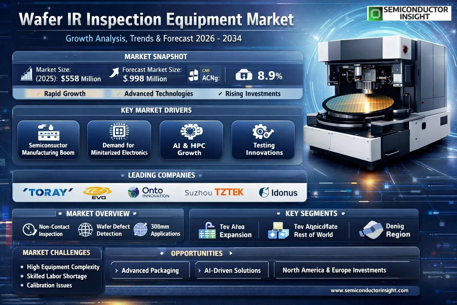
Global Wafer IR Inspection Equipment market size was valued at USD 558 million in 2025. The market is projected to grow from USD 1.28 billion in 2025 to USD 2.32 billion by 2034, exhibiting a CAGR of 8.9% during the forecast period.
Wafer automatic infrared inspection equipment is an important tool for non-contact temperature measurement and defect detection in the semiconductor industry. These devices use the principle of infrared radiation to accurately measure the temperature of the wafer surface and identify various defects that may occur in the wafer during the production process.
The market is experiencing rapid growth due to several factors, including increased investment in semiconductor manufacturing, rising demand for advanced inspection technologies, and the increasing prevalence of miniaturized electronic components. Additionally, the growing demand for and advancements in testing technologies such as artificial intelligence and machine learning are contributing to market expansion. Initiatives by key players in the market are also expected to fuel market growth. For instance, in February 2024, Onto Innovation Inc. collaborated with a leading semiconductor manufacturer to develop next-generation IR inspection solutions. Toray Engineering, EV Group, Suzhou TZTEK, Idonus Sarl, YAYATECH Co. Ltd, Jiangxi Lionhearted, and Nutrim Technology are some of the key players that operate in the market with a wide range of portfolios.
MARKET DRIVERS
Advancements in Advanced Semiconductor Nodes
Wafer IR Inspection Equipment Market is propelled by the relentless push toward smaller process nodes like 3nm and below, where infrared inspection becomes essential for detecting subsurface defects invisible to optical systems. Leading foundries are ramping up production capacity, driving demand for high-resolution IR tools that ensure yield improvements of up to 15% in advanced packaging processes.
Growth in AI and High-Performance Computing
Explosive growth in AI chips and data center processors necessitates precise wafer-level defect detection, boosting adoption of IR inspection equipment. With global semiconductor sales projected to exceed $600 billion by 2025, the market benefits from increased fab investments, particularly in Asia-Pacific regions.
➤ IR systems enable non-contact backside inspection, reducing contamination risks and supporting heterogeneous integration trends in Wafer IR Inspection Equipment Market.
Additionally, the rise of electric vehicles and 5G infrastructure amplifies the need for reliable supply chains, further accelerating equipment deployments across major manufacturers.
MARKET CHALLENGES
Technical Integration and Calibration Hurdles
Integrating IR inspection tools into existing fab workflows poses significant challenges due to varying wafer materials and thicknesses, often requiring custom calibrations that extend setup times by 20-30%. Compatibility issues with legacy systems hinder seamless adoption in Wafer IR Inspection Equipment Market.
Other Challenges
Skilled labor shortages for operating advanced IR systems exacerbate throughput delays, while thermal noise interference in high-volume production environments demands ongoing R&D investments.
High Equipment Complexity
Sophisticated algorithms for real-time defect classification increase maintenance costs, with annual servicing accounting for nearly 10% of total ownership expenses in mature facilities.
MARKET RESTRAINTS
Supply Chain Vulnerabilities
Geopolitical tensions and raw material shortages, particularly for specialized IR sensors, constrain Wafer IR Inspection Equipment Market growth, leading to lead times extending up to 12 months for critical components. This impacts scaling in new fab constructions globally.
High capital expenditures, often exceeding $5 million per unit, limit accessibility for smaller fabs, concentrating market share among top-tier players like TSMC and Samsung.
Regulatory compliance for cleanroom standards and export controls on high-tech optics further slows deployment, especially in emerging semiconductor hubs.
MARKET OPPORTUNITIES
Expansion into Advanced Packaging and 3D Integration
The shift toward chiplet designs and 3D stacking opens vast opportunities in Wafer IR Inspection Equipment Market, where IR tools excel in void and delamination detection, potentially capturing 25% additional market share by 2028.
Growing investments in Europe and North America for domestic semiconductor production provide avenues for localized manufacturing and service networks.
Innovations in AI-enhanced IR imaging promise throughput gains of 40%, attracting partnerships with equipment vendors and positioning the market for sustained double-digit CAGR through the decade.
Wafer IR Inspection Equipment Market Trends
Advancements in Fully-Automatic Systems
In Wafer IR Inspection Equipment Market, the shift toward fully-automatic systems represents a pivotal trend driven by the semiconductor industry’s need for higher precision and throughput. These systems leverage infrared radiation for non-contact temperature measurement and defect detection on wafer surfaces, enabling real-time identification of production anomalies without physical contact. This transition enhances yield rates and reduces downtime, as manufacturers integrate advanced IR sensors that detect subsurface defects invisible to traditional optical methods. Industry surveys indicate that fully-automatic equipment is gaining prominence due to its compatibility with high-volume manufacturing environments.
Other Trends
Regional Market Expansion
Asia, particularly China, Japan, and South Korea, is witnessing accelerated growth in Wafer IR Inspection Equipment Market, fueled by robust semiconductor fabrication investments. These regions dominate due to expansive production capacities for logic and memory chips, where IR inspection tools are essential for maintaining wafer integrity. North America and Europe follow, with key players focusing on innovation to meet stringent quality standards in advanced nodes.
Rising Demand for 300mm Wafer Applications
Wafer IR Inspection Equipment Market is experiencing heightened demand for applications tailored to 300mm wafers, as semiconductor producers scale up for cost efficiency and performance gains. This trend aligns with the evolution toward larger wafer formats, where IR technology excels in monitoring thermal profiles and identifying microcracks or contamination during processing. Leading manufacturers such as Toray, EV Group, Onto Innovation Inc, Suzhou TZTEK, and YAYATECH Co. Ltd are developing specialized solutions, intensifying competition and spurring technological refinements. Additionally, semi-automatic systems continue to serve niche applications, but the market favors automation for 200mm and larger wafers to support next-generation device fabrication.
COMPETITIVE LANDSCAPE
Key Industry Players
Wafer IR Inspection Equipment Market Overview
Wafer IR Inspection Equipment Market is dominated by a few leading players, with Global top five companies holding a significant revenue share as of 2025. Key leaders include Onto Innovation Inc. and EV Group, which leverage advanced infrared technology for non-contact defect detection and temperature measurement in semiconductor wafer production. The market structure is moderately concentrated, driven by high barriers to entry due to technological complexity and precision requirements. Valued at US$558 million in 2025, the sector is projected to grow to US$998 million by 2034 at a CAGR of 8.9%, fueled by demand for fully-automatic systems in 200mm and 300mm wafer applications.
Beyond the top tier, niche players like Suzhou TZTEK, Idonus Sarl, and YAYATECH Co. Ltd contribute through specialized offerings in semi-automatic and custom IR inspection solutions, targeting regional markets in Asia and Europe. Emerging Chinese firms such as Jiangxi Lionhearted and Nutrim Technology are gaining traction with cost-effective innovations, intensifying competition. Toray provides integrated solutions combining IR inspection with materials expertise. This fragmented landscape encourages strategic partnerships and R&D investments to address challenges like yield optimization in advanced nodes.
List of Key Wafer IR Inspection Equipment Companies Profiled
- Toray
- EV Group
- Onto Innovation Inc
- Suzhou TZTEK
- Idonus Sarl
- YAYATECH Co. Ltd
- Jiangxi Lionhearted
- Nutrim Technology
- KLA Corporation
- Hitachi High-Tech
- Camtek Ltd
- CyberOptics (Nordson)
- Applied Materials
- ASML Holding
- Lam Research
Segment Analysis:
| Segment Category | Sub-Segments | Key Insights |
| By Type |
|
Fully-automatic
|
| By Application |
|
300mm Wafer
|
| By End User |
|
Foundries
|
| By Deployment |
|
Inline Inspection
|
| By Wafer Material |
|
Silicon Wafers
|
Regional Analysis: Wafer IR Inspection Equipment Market
Asia-Pacific
Semiconductor powerhouses in Asia-Pacific drive Wafer IR Inspection Equipment Market through expansive cleanroom facilities. These hubs prioritize IR systems for real-time defect mapping, vital for advanced packaging and 3D stacking. Proximity to raw material sources and assembly lines streamlines deployment, reducing latency in production feedback loops and elevating overall equipment effectiveness.
Intense research activities in Asia-Pacific accelerate innovations in Wafer IR Inspection Equipment Market offerings. Collaborations between academia and industry yield hyperspectral IR imaging advancements, improving sensitivity to nanoscale anomalies. This focus supports rapid iteration of inspection protocols, aligning with evolving node shrinks and heterogeneous integration demands.
High adoption rates characterize the Asia-Pacific Wafer IR Inspection Equipment Market, with fabs integrating these tools early in process development. Emphasis on high-throughput inline monitoring enhances throughput without compromising quality, particularly for power devices and photonics. Ecosystem maturity enables seamless upgrades to AI-enhanced IR analytics.
Supply chain vulnerabilities pose challenges in the Asia-Pacific Wafer IR Inspection Equipment Market, prompting diversification efforts. Skill gaps in advanced IR data interpretation are being addressed through targeted training programs, ensuring sustained operational excellence amid aggressive capacity ramps.
North America
North America plays a pivotal role in Wafer IR Inspection Equipment Market, anchored by pioneering semiconductor design centers and equipment innovators. The region excels in developing cutting-edge IR sensor technologies, which are then deployed globally. Strong emphasis on advanced packaging and heterogeneous integration fuels demand for sophisticated inspection capabilities to detect hidden voids and cracks. Collaborative ecosystems involving IDMs and OSATs prioritize precision metrology, enhancing yield optimization. Business strategies here focus on software-hardware synergies, incorporating machine learning for predictive maintenance. Despite manufacturing shifts abroad, North America’s R&D leadership ensures influence over Wafer IR Inspection Equipment Market standards and future roadmaps.
Europe
Europe contributes significantly to Wafer IR Inspection Equipment Market through its specialized compound semiconductor sector and automotive chip production. Precision engineering traditions drive adoption of high-resolution IR systems for power electronics and sensors. Regulatory frameworks emphasize sustainability, pushing innovations in energy-efficient inspection tools. Key players leverage regional consortia to address challenges in legacy node scaling and SiC/GaN processes. Wafer IR Inspection Equipment Market here benefits from cross-border collaborations, fostering customized solutions that align with stringent quality benchmarks and diversified supply strategies.
South America
South America is an emerging player in Wafer IR Inspection Equipment Market, with growing electronics assembly and nascent fab investments. Brazil leads regional efforts, focusing on cost-effective IR inspection for consumer devices and renewables. Infrastructure developments support technology transfer from global leaders, aiding defect reduction in volume production. Challenges include talent development, yet strategic partnerships promise acceleration. Wafer IR Inspection Equipment Market dynamics reflect optimism, with emphasis on affordable, scalable solutions to build local capabilities.
Middle East & Africa
The Middle East & Africa region advances in Wafer IR Inspection Equipment Market via diversification from oil into tech fabrication hubs. UAE and Israel’s initiatives target photonics and defense applications, demanding robust IR inspection for exotic materials. Investments in training and infrastructure mitigate adoption barriers. Regional Wafer IR Inspection Equipment Market growth hinges on international alliances, enabling access to state-of-the-art tools while nurturing indigenous expertise for long-term resilience.
Report Scope
This market research report provides a comprehensive analysis of Wafer IR Inspection Equipment Market, covering the forecast period 2026–2034. It offers detailed insights into market dynamics, technological advancements, competitive landscape, and key trends shaping the industry.
Key focus areas of the report include:
- Market Overview: The report begins with an overview outlining its current market scenario, key growth indicators, and industry transformation drivers. It discusses macroeconomic factors, demand–supply balance, regulatory landscape, and the strategic role of semiconductors in powering advancements across industries such as automotive, telecommunications, consumer electronics, and industrial automation.
- Market Size & Forecast: Historical data and future projections for revenue, unit shipments, and market value across major regions and segments.
- Segmentation Analysis: Detailed breakdown by product type, technology, application, and end-user industry to identify high-growth segments and investment opportunities.
- Regional Insights: Insights into market performance across North America, Europe, Asia-Pacific, Latin America, and the Middle East & Africa, including country-level analysis where relevant.
- Competitive Landscape: Profiles of leading market participants, including their product offerings, R&D focus, manufacturing capacity, pricing strategies, and recent developments such as mergers, acquisitions, and partnerships.
- Technology Trends & Innovation: Assessment of emerging technologies, integration of AI/IoT, semiconductor design trends, fabrication techniques, and evolving industry standards.
- Market Drivers & Restraints: Evaluation of factors driving market growth along with challenges, supply chain constraints, regulatory issues, and market-entry barriers.
- Stakeholder Insights: Insights for component suppliers, OEMs, system integrators, investors, and policymakers regarding the evolving ecosystem and strategic opportunities.
Primary and secondary research methods are employed, including interviews with industry experts, data from verified sources, and real-time market intelligence to ensure the accuracy and reliability of the insights presented.
FREQUENTLY ASKED QUESTIONS:
What is the current market size of Wafer IR Inspection Equipment Market?
-> Global Wafer IR Inspection Equipment market was valued at USD 558 million in 2025 and is expected to reach USD 998 million by 2034, at a CAGR of 8.9% during the forecast period.
Which key companies operate in Wafer IR Inspection Equipment Market?
-> Key players include Toray, EV Group, Onto Innovation Inc, Suzhou TZTEK, Idonus Sarl, YAYATECH Co. Ltd, Jiangxi Lionhearted, Nutrim Technology, etc.
What are the key growth drivers?
-> Key growth drivers include demand for non-contact temperature measurement and defect detection in semiconductor wafer production.
Which region dominates the market?
-> Asia dominates the market, with key countries including China, Japan, and South Korea.
What are the emerging trends?
-> Emerging trends include fully-automatic equipment, applications for 300mm wafers, and advancements in infrared defect detection technologies.

Get Sample Report PDF for Exclusive Insights
Report Sample Includes
- Table of Contents
- List of Tables & Figures
- Charts, Research Methodology, and more...
 Download Sample Report PDF