Market Insights
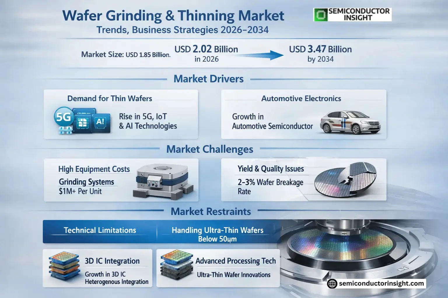
Global Wafer Grinding & Thinning Market size was valued at USD 1.85 billion in 2025. The market is projected to grow from USD 2.02 billion in 2026 to USD 3.47 billion by 2034, exhibiting a CAGR of 7.1% during the forecast period.
Wafer grinding and thinning are critical semiconductor manufacturing processes that reduce wafer thickness while maintaining structural integrity for advanced packaging and miniaturized electronic devices. These techniques involve precision mechanical or chemical-mechanical polishing (CMP) to achieve ultra-thin wafers required for applications such as MEMS, power devices, and 3D IC integration.
The market growth is driven by increasing demand for compact electronic components across consumer electronics, automotive systems, and data centers. While the transition to larger 300mm wafers presents technical challenges in thinning processes, advancements in equipment automation and hybrid grinding-CMP solutions are creating new opportunities. Key players like DISCO Corporation and Axus Technology continue to innovate with improved throughput and yield-enhancing technologies to meet evolving industry requirements.
MARKET DRIVERS
Growing Demand for Thin Wafers in Semiconductor Industry
Wafer Grinding & Thinning Market is experiencing significant growth due to the rising demand for thinner wafers in advanced semiconductor manufacturing. As chip designs become more complex and compact, manufacturers require ultra-thin wafers to meet performance and space-saving requirements. The increasing adoption of 5G, IoT, and AI technologies further drives this demand.
Expansion of Automotive Electronics
Automotive electrification and autonomous driving technologies are fueling demand for high-performance semiconductor devices, which rely on precision wafer grinding and thinning processes. The automotive semiconductor market is projected to grow at approximately 8% annually, directly benefiting the Wafer Grinding & Thinning Market.
The trend toward wafer-level packaging continues to accelerate, with over 15% of advanced packaging now utilizing some form of wafer thinning technology to enable higher-density interconnects.
MARKET CHALLENGES
High Equipment and Process Costs
Wafer Grinding & Thinning Market faces significant challenges from the high capital expenditure required for advanced grinding equipment. Precision thinning systems can cost upwards of USD 1 million per unit, creating barriers for smaller manufacturers.
Other Challenges
Yield and Quality Control Issues
Maintaining wafer integrity during thinning processes remains a critical challenge, with breakage rates averaging 2-3% in production environments despite technological advancements.
MARKET RESTRAINTS
Technical Limitations in Ultra-Thin Wafer Handling
As wafers become thinner (below 50μm), handling and processing challenges increase significantly. The fragility of ultra-thin wafers limits the pace of adoption in some applications, particularly where mechanical stress tolerance is critical.
MARKET OPPORTUNITIES
Emerging 3D IC and Heterogeneous Integration Trends
Wafer Grinding & Thinning Market stands to benefit from the growing adoption of 3D IC packaging and heterogeneous integration techniques. These advanced packaging approaches require precise wafer thinning to achieve optimal stack heights and thermal performance.
Wafer Grinding & Thinning Market Trends
Advancements in Ultra-Thin Wafer Processing Technologies
The semiconductor industry is witnessing significant progress in wafer grinding and thinning techniques to meet the demand for ultra-thin wafers below 100μm. Leading manufacturers are investing in advanced grinding equipment with improved precision control systems to minimize wafer breakage and improve yield rates.
Other Trends
Regional Market Growth Patterns
Asia-Pacific continues to dominate the Wafer Grinding & Thinning Market, driven by semiconductor manufacturing hubs in China, Taiwan, and South Korea. North America maintains strong demand from advanced computing applications, while Europe shows steady growth in automotive semiconductor applications.
Increasing Adoption in Next-Generation Applications
Wafer grinding and thinning technologies are becoming critical for emerging applications including advanced memory devices, 5G communications, and power semiconductors. The rise of 3D IC packaging and through-silicon via (TSV) technologies is creating new demand for precision thinning services in the semiconductor industry.
Material Innovation Driving Process Improvements
New grinding wheel materials and bonding technologies are being developed to achieve better surface finishes and reduce subsurface damage. Temporary bonding and debonding solutions are also evolving to handle thinner wafers during the grinding process without compromising structural integrity.
Market Consolidation Among Key Players
The competitive landscape of the Wafer Grinding & Thinning Market shows increasing consolidation with major players like DISCO Corporation and Syagrus Systems expanding their service capabilities through strategic partnerships and technological acquisitions to offer comprehensive foundry solutions.
COMPETITIVE LANDSCAPE
Key Industry Players
Global Wafer Grinding & Thinning Market Leaders and Disruptors
Wafer Grinding & Thinning Market is dominated by specialized semiconductor equipment manufacturers, with DISCO Corporation and AXUS Technology leading global market share due to their advanced precision grinding systems. These established players maintain strong R&D capabilities, particularly in ultra-thin wafer processing below 100μm thickness, serving major semiconductor fabs worldwide. The top five companies collectively accounted for approximately 40% of the 2025 market revenue, with Japanese and American firms showing particular strength in high-end thinning technologies.
A growing segment of mid-sized specialists like SIEGERT WAFER GmbH and Optim Wafer Services are gaining traction through niche capabilities in compound semiconductor processing and MEMS wafer thinning. Chinese manufacturers including Huahong Group and MACMIC are expanding rapidly, supported by domestic semiconductor industry growth and government initiatives, though still trailing in cutting-edge thin wafer technologies below 50μm thickness where Japanese and German firms maintain leadership.
List of Key Wafer Grinding & Thinning Companies Profiled
- DISCO Corporation
- AXUS TECHNOLOGY
- Syagrus Systems
- Optim Wafer Services
- Silicon Valley Microelectronics, Inc.
- SIEGERT WAFER GmbH
- NICHIWA KOGYO CO.,LTD.
- Integra Technologies
- Valley Design
- Helia Photonics
- Aptek Industries
- UniversityWafer, Inc.
- Micross
- Power Master Semiconductor Co., Ltd.
- Enzan Factory Co., Ltd.
Segment Analysis:
| Segment Category | Sub-Segments | Key Insights |
| By Type |
|
Ultra-Thin Wafers segment demonstrates higher growth potential due to:
|
| By Application |
|
Consumer Electronics maintains leadership with critical factors including:
|
| By End User |
|
IDMs (Integrated Device Manufacturers) show significant adoption due to:
|
| By Technology |
|
Chemical Mechanical Polishing emerges as preferred technology because:
|
| By Wafer Size |
|
300mm (12-inch) wafers dominate the market owing to:
|
Regional Analysis: Wafer Grinding & Thinning Market
Asia-Pacific
Taiwan houses the world’s most advanced foundries that push wafer thinning requirements below 50μm. The TSMC ecosystem drives innovation in ultra-thin wafer handling solutions and temporary bonding technologies for 3D IC packaging applications.
South Korean memory manufacturers require specialized grinding solutions for NAND flash and DRAM production. The market sees increasing adoption of automated wafer thinning systems to handle fragile memory wafers with higher throughput requirements.
China’s semiconductor self-sufficiency drive has created demand for domestic wafer thinning equipment. Local players are developing alternative solutions amid technology export restrictions, focusing on backend process innovations for mature nodes.
Southeast Asian nations are developing wafer-level packaging capabilities, with Malaysia and Singapore becoming important hubs for outsourced semiconductor assembly and test operations requiring thinning services.
North America
North America remains a critical innovation center for wafer grinding technologies, particularly for advanced packaging applications. The region’s IDMs and fabless companies drive demand for ultra-thin wafer solutions below 100μm thickness. Research institutions collaborate with equipment manufacturers to develop novel thinning techniques for heterogeneous integration. The U.S. CHIPS Act is stimulating investments in domestic advanced packaging capabilities that will require next-generation wafer thinning solutions.
Europe
Europe’s Wafer Grinding & Thinning Market benefits from strong automotive and industrial semiconductor demand. German and French equipment manufacturers lead in precision grinding systems for power electronics and MEMS applications. The region shows growing interest in wafer thinning solutions for silicon carbide and gallium nitride power devices, supported by substantial R&D funding for power electronics advancements.
Middle East & Africa
The Middle East is witnessing emerging wafer thinning requirements as nations diversify technology investments. Saudi Arabia’s semiconductor initiatives and Israel’s fabless ecosystem create new opportunities. Africa’s market remains nascent but shows potential for basic wafer processing capabilities to support local electronics manufacturing growth.
South America
South America’s wafer grinding market primarily serves regional electronics assembly needs. Brazil leads in semiconductor packaging capabilities, importing thinning equipment for discrete devices and basic ICs. The region shows potential for growth as automotive electronics manufacturing expands across Mexico and Brazil.
Report Scope
This market research report provides a comprehensive analysis of the Wafer Grinding & Thinning Market, covering the forecast period 2025–2034. It offers detailed insights into market dynamics, technological advancements, competitive landscape, and key trends shaping the industry.
Key focus areas of the report include:
- Market Overview: The report begins with an overview outlining its current market scenario, key growth indicators, and industry transformation drivers. It discusses macroeconomic factors, demand–supply balance, regulatory landscape, and the strategic role of semiconductors in powering advancements across industries such as automotive, telecommunications, consumer electronics, and industrial automation.
- Market Size & Forecast: Historical data and future projections for revenue, unit shipments, and market value across major regions and segments.
- Segmentation Analysis: Detailed breakdown by product type, technology, application, and end-user industry to identify high-growth segments and investment opportunities.
- Regional Insights: Insights into market performance across North America, Europe, Asia-Pacific, Latin America, and the Middle East & Africa, including country-level analysis where relevant.
- Competitive Landscape: Profiles of leading market participants, including their product offerings, R&D focus, manufacturing capacity, pricing strategies, and recent developments such as mergers, acquisitions, and partnerships.
- Technology Trends & Innovation: Assessment of emerging technologies, integration of AI/IoT, semiconductor design trends, fabrication techniques, and evolving industry standards.
- Market Drivers & Restraints: Evaluation of factors driving market growth along with challenges, supply chain constraints, regulatory issues, and market-entry barriers.
- Stakeholder Insights: Insights for component suppliers, OEMs, system integrators, investors, and policymakers regarding the evolving ecosystem and strategic opportunities.
Primary and secondary research methods are employed, including interviews with industry experts, data from verified sources, and real-time market intelligence to ensure the accuracy and reliability of the insights presented.
FREQUENTLY ASKED QUESTIONS:
What is the current market size of Wafer Grinding & Thinning Market?
-> Wafer Grinding & Thinning Market size was valued at USD 1.85 billion in 2025. The market is projected to grow from USD 2.02 billion in 2026 to USD 3.47 billion by 2034, exhibiting a CAGR of 7.1% during the forecast period.
Which key companies operate in Wafer Grinding & Thinning Market?
-> Key players include Syagrus Systems, Optim Wafer Services, Silicon Valley Microelectronics, Inc., SIEGERT WAFER GmbH, NICHIWA KOGYO CO.,LTD., Integra Technologies, Valley Design, AXUS TECHNOLOGY, Helia Photonics, and DISCO Corporation, among others. In 2025, the global top five players had approximately % market share.
What are the key growth drivers?
-> Key growth drivers include increasing demand for miniaturized semiconductor components, advancements in wafer thinning technologies, and growth in consumer electronics and automotive electronics sectors.
Which region dominates the market?
-> Asia-Pacific dominates the market with China projected to reach USD million by 2034. The U.S. market was estimated at USD million in 2025.
What are the key market segments?
-> Key segments include Ordinary Wafers and Ultra-Thin Wafers by product type, and Consumer Electronics, Automotive Electronics, Computer and Data Center, and Others by application.
What is the growth outlook for Ordinary Wafers segment?
-> Ordinary Wafers segment will reach USD million by 2034, with a % CAGR in next six years.
Get Sample Report PDF for Exclusive Insights
Report Sample Includes
- Table of Contents
- List of Tables & Figures
- Charts, Research Methodology, and more...
 Download Sample Report PDF