
Wafer Edge Profiler Market Insights
Global Wafer Edge Profiler market was valued at USD 572 million in 2025. The market is projected to reach USD 825 million by 2034, exhibiting a CAGR of 5.5% during the forecast period.
A Wafer Edge Profiler is a specialized metrology tool used in the semiconductor manufacturing industry to measure and analyze the edge profile of semiconductor wafers. The edge profile of a wafer is critical for ensuring high yields in semiconductor fabrication processes, as irregularities or defects at the edge can lead to issues like wafer breakage, poor coating uniformity, or contamination.
The market is experiencing steady growth due to surging demand for advanced semiconductors driven by AI, 5G, and electric vehicles. Furthermore, expansions in wafer fabrication facilities worldwide and the shift toward larger wafer sizes like 12 inches are fueling adoption. Key players such as KLA Corporation, Onto Innovation, KoCoS Technology Group, Lasertec Corporation, and Hitachi High-Tech dominate with innovative contactless and contact solutions. Recent developments include enhanced optical profiling technologies for sub-3nm nodes, supporting higher precision in edge metrology.
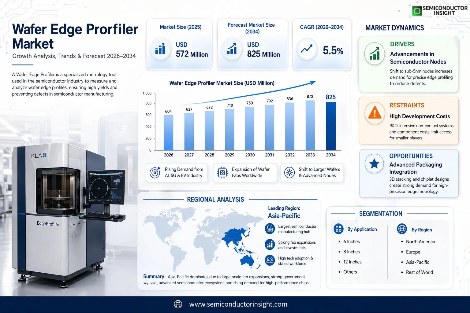
MARKET DRIVERS
Advancements in Semiconductor Nodes
Wafer Edge Profiler Market is propelled by the shift toward sub-5nm process nodes in semiconductor fabrication. Precision edge profiling ensures wafer uniformity, reducing defects in advanced chips for AI and 5G applications. With global semiconductor sales reaching approximately $600 billion in 2023, demand for high-accuracy tools has surged.
Growth in Electronics and EVs
Expansion in electric vehicles and consumer electronics drives the need for reliable wafer edge metrology. Manufacturers like TSMC and Samsung invest heavily in wafer fab equipment, where edge profilers play a critical role in yield optimization. The market benefits from a projected 9% CAGR in wafer fabrication equipment through 2028.
➤ Edge profilers enable 99.5% yield improvements in edge defect detection, supporting high-volume production for data center chips.
Increasing fab capacity in Asia-Pacific further accelerates adoption, as precise edge control becomes essential for stacking and packaging technologies.
MARKET CHALLENGES
High Development Costs
Wafer Edge Profiler Market faces hurdles from the substantial R&D investments required for non-contact, high-resolution systems. Integrating laser interferometry with AI-driven analysis elevates costs, challenging smaller players amid a competitive landscape dominated by established firms.
Other Challenges
Calibration complexities in diverse wafer materials, from silicon to compound semiconductors, complicate deployment. Variability in edge geometries across 200mm to 450mm wafers demands versatile yet precise instrumentation.
Supply Chain Volatility
Geopolitical tensions and raw material shortages disrupt component availability for optical sensors, impacting delivery timelines and escalating prices by up to 15% in recent years.Skill shortages in metrology expertise slow adoption rates in emerging fabs.
MARKET RESTRAINTS
Regulatory and Standardization Gaps
Stringent semiconductor industry standards, coupled with evolving cleanroom protocols, restrain rapid market expansion for wafer edge profilers. Compliance with SEMI guidelines requires ongoing validation, increasing time-to-market.High capital intensity limits access for mid-tier foundries, with systems costing over $500,000 per unit. Economic slowdowns in key regions further dampen investments.Competition from alternative metrology tools, like acoustic profiling, poses substitution risks despite superior accuracy of optical edge profilers.Intellectual property barriers slow innovation diffusion across Wafer Edge Profiler Market.
MARKET OPPORTUNITIES
Advanced Packaging Integration
Wafer Edge Profiler Market holds potential in heterogeneous integration and 3D stacking, where edge precision is vital for fan-out and chiplet designs. This aligns with a forecasted 12% growth in advanced packaging revenues by 2027.Emerging EUV lithography extensions demand sub-micron edge control, opening avenues for next-gen profilers with real-time analytics.Expansion into photonics and power semiconductors offers untapped demand, particularly in Europe and North America fabs.AI-enhanced profilers could capture 25% market share by automating defect classification.
Wafer Edge Profiler Market Trends
Rising Adoption of Contactless Profilers
In Wafer Edge Profiler Market, contactless measurement technologies are gaining prominence due to their non-destructive nature, enabling precise edge profile analysis without risking wafer damage. Semiconductor manufacturers prioritize these tools to detect irregularities at the wafer edge, which can cause breakage, uneven coatings, or contamination during fabrication. This shift supports higher yields in advanced processes, as contactless systems use optical or laser-based methods for accurate profiling. Industry surveys indicate that contactless segments are expanding as fabs transition to finer nodes requiring superior edge quality control.
Other Trends
Growth in Larger Wafer Applications
Demand for wafer edge profilers tailored to 12-inch and 8-inch wafers is accelerating within Wafer Edge Profiler Market, driven by the semiconductor industry’s move toward larger substrates for cost-efficient production of high-performance chips. These sizes dominate applications in logic and memory fabrication, where edge precision directly impacts process reliability. Tools optimized for these diameters help mitigate defects amplified by scale, fostering adoption across foundries and IDMs globally.
Intensifying Competition and Regional Shifts
Wafer Edge Profiler Market features robust competition from key players such as KLA Corporation, Onto Innovation, and Lasertec Corporation, with top manufacturers focusing on innovation in measurement accuracy and integration with inline metrology suites. Asia, particularly China, Japan, and South Korea, emerges as a pivotal growth hub, supported by expanding semiconductor capacity and investments in domestic supply chains. European and North American markets emphasize high-end contactless solutions, while surveys highlight challenges like supply chain obstacles and the need for standardized edge profiling protocols. Overall, these dynamics position Wafer Edge Profiler Market for sustained evolution aligned with global fab expansions and technological advancements in yield optimization.
COMPETITIVE LANDSCAPE
Key Industry Players
Leading Manufacturers and Market Share Dynamics in Wafer Edge Profiler Sector
Wafer Edge Profiler Market exhibits a concentrated structure dominated by a few established leaders, with KLA Corporation and Onto Innovation commanding the largest shares due to their advanced metrology solutions and extensive semiconductor industry presence. These top players leverage cutting-edge contactless technologies to ensure precise edge profile measurements, critical for high-yield wafer fabrication across 6-, 8-, and 12-inch applications. In 2025, the global top five manufacturers collectively accounted for a substantial revenue portion in a market valued at $572 million, fostering intense competition focused on innovation, R&D investment, and integration with broader fab processes amid a projected CAGR of 5.5% to $825 million by 2034.
Beyond the frontrunners, niche players like Lasertec Corporation, Hitachi High-Tech, and KoCoS Technology Group provide specialized contact and contactless systems, targeting edge defect analysis and contamination prevention in high-volume manufacturing. Emerging Asian firms such as Xinmao Semiconductor Technology, Jiangsu Jinggong Semiconductor Equipment, and Suzhou Secote Precision Electronic are gaining traction with cost-effective solutions tailored for regional demand in China and Japan. This mix of incumbents and challengers drives market evolution, with strategic mergers, product enhancements, and expansions into larger wafer sizes shaping the competitive landscape.
List of Key Wafer Edge Profiler Companies Profiled
- KLA Corporation
- Onto Innovation
- KoCoS Technology Group
- Lasertec Corporation
- HOLOGENIX
- Optima Co., Ltd.
- Delta Electronics
- Hitachi High-Tech
- ERS
- Xinmao Semiconductor Technology
- Jiangsu Jinggong Semiconductor Equipment
- Suzhou Secote Precision Electronic
- Beijing Khltech Semiconductor Technology
Segment Analysis:
| Segment Category | Sub-Segments | Key Insights |
| By Type |
|
Contactless
|
| By Application |
|
12 Inches
|
| By End User |
|
Foundries
|
| By Deployment Mode |
|
Inline
|
| By Industry Vertical |
|
Logic Semiconductors
|
Regional Analysis: Wafer Edge Profiler Market
Asia-Pacific
Taiwan anchors Asia-Pacific leadership with world-class foundries demanding high-precision wafer edge profilers. Advanced nodes require meticulous edge geometry control to prevent chipping during handling. Local integration of profilers into fab workflows boosts throughput, supported by a mature supplier network. Innovations in optical sensing technologies cater to diverse wafer sizes, reinforcing regional market strength.
South Korea excels in memory chip production, where wafer edge profilers ensure uniform profiles vital for stacking technologies. Leading firms prioritize non-destructive measurement tools, enhancing defect detection. The emphasis on high-volume manufacturing drives profiler customization, with R&D emphasizing automation for 24/7 operations, solidifying Asia-Pacific’s edge.
China’s aggressive fab buildout amplifies Wafer Edge Profiler Market growth, focusing on domestic supply security. Profilers adapted for large-diameter wafers support 3D NAND and logic scaling. Policy-driven investments spur indigenous development, improving edge metrology accuracy and integration with AI analytics for predictive maintenance.
Asia-Pacific’s interconnected ecosystem streamlines wafer edge profiler deployment, from design to fab floors. Cross-border collaborations yield hybrid systems combining laser and white-light interferometry. This synergy accelerates market penetration, addressing evolving needs in power semiconductors and photonics with tailored solutions.
North America
North America plays a crucial role in Wafer Edge Profiler Market through innovation and equipment leadership. Home to pioneering metrology firms, the region excels in developing next-generation profilers with atomic-level precision for R&D labs. While domestic fabrication lags, demand arises from design houses and pilot lines in advanced packaging. Strategic alliances with Asian partners facilitate technology transfer, emphasizing software enhancements for data analytics. The focus on sustainable practices integrates eco-friendly materials in profiler construction, positioning North America as a quality benchmark despite volume constraints.
Europe
Europe contributes to Wafer Edge Profiler Market via specialized research and high-value applications. Precision engineering hubs develop hybrid profilers for automotive and aerospace semiconductors, prioritizing robustness in harsh environments. Collaborative EU projects advance edge defect classification algorithms, aiding yield optimization. Though manufacturing scale is modest, the region’s strength lies in regulatory-compliant standards driving profiler reliability. Emerging quantum computing initiatives spur demand for ultra-precise tools, fostering steady market evolution.
South America
South America represents an emerging frontier in Wafer Edge Profiler Market, with nascent semiconductor efforts tied to electronics assembly. Limited fab infrastructure focuses demand on imported profilers for quality assurance in consumer devices. Regional growth hinges on workforce upskilling and foreign investments, targeting edge profiling for cost-sensitive production. Potential in renewable energy electronics encourages basic metrology adoption, laying groundwork for expanded capabilities amid infrastructural challenges.
Middle East & Africa
The Middle East & Africa region shows gradual uptake in Wafer Edge Profiler Market, linked to diversification from oil dependency. Pilot semiconductor zones in the UAE and South Africa employ profilers for display and sensor wafers. Emphasis on localized training builds expertise, while partnerships import advanced tools for edge yield improvement. Harsh climates necessitate ruggedized designs, positioning the area for incremental gains as digital transformation accelerates.
Report Scope
This market research report provides a comprehensive analysis of the Wafer Edge Profiler Market , covering the forecast period 2026–2034. It offers detailed insights into market dynamics, technological advancements, competitive landscape, and key trends shaping the industry.
Key focus areas of the report include:
- Market Overview: The report begins with an overview outlining its current market scenario, key growth indicators, and industry transformation drivers. It discusses macroeconomic factors, demand–supply balance, regulatory landscape, and the strategic role of semiconductors in powering advancements across industries such as automotive, telecommunications, consumer electronics, and industrial automation.
- Market Size & Forecast: Historical data and future projections for revenue, unit shipments, and market value across major regions and segments.
- Segmentation Analysis: Detailed breakdown by product type, technology, application, and end-user industry to identify high-growth segments and investment opportunities.
- Regional Insights: Insights into market performance across North America, Europe, Asia-Pacific, Latin America, and the Middle East & Africa, including country-level analysis where relevant.
- Competitive Landscape: Profiles of leading market participants, including their product offerings, R&D focus, manufacturing capacity, pricing strategies, and recent developments such as mergers, acquisitions, and partnerships.
- Technology Trends & Innovation: Assessment of emerging technologies, integration of AI/IoT, semiconductor design trends, fabrication techniques, and evolving industry standards.
- Market Drivers & Restraints: Evaluation of factors driving market growth along with challenges, supply chain constraints, regulatory issues, and market-entry barriers.
- Stakeholder Insights: Insights for component suppliers, OEMs, system integrators, investors, and policymakers regarding the evolving ecosystem and strategic opportunities.
Primary and secondary research methods are employed, including interviews with industry experts, data from verified sources, and real-time market intelligence to ensure the accuracy and reliability of the insights presented.
FREQUENTLY ASKED QUESTIONS:
What is the current market size of Wafer Edge Profiler Market?
-> Global Wafer Edge Profiler market was valued at USD 572 million in 2025 and is expected to reach USD 825 million by 2034, at a CAGR of 5.5% during the forecast period.
Which key companies operate in Wafer Edge Profiler Market?
-> Key players include KLA Corporation, Onto Innovation, KoCoS Technology Group, Lasertec Corporation, HOLOGENIX, Optima Co., Ltd., Delta Electronics, Hitachi High-Tech, ERS, Xinmao Semiconductor Technology, among others.
What are the key growth drivers?
-> Key growth drivers include demand for high-yield semiconductor fabrication, advancements in wafer edge metrology to prevent breakage and contamination, and expansion of semiconductor manufacturing.
Which region dominates the market?
-> Asia dominates the market, with key contributions from China, Japan, and South Korea, while North America, led by the U.S., holds significant share.
What are the emerging trends?
-> Emerging trends include shift towards contactless profiling technologies, support for larger wafer sizes such as 12 inches, and integration with advanced semiconductor processes.

Get Sample Report PDF for Exclusive Insights
Report Sample Includes
- Table of Contents
- List of Tables & Figures
- Charts, Research Methodology, and more...
 Download Sample Report PDF



