MARKET INSIGHTS
The global Wafer Boat Market size was valued at US$ 234 million in 2024 and is projected to reach US$ 378 million by 2032, at a CAGR of 7.0% during the forecast period 2025-2032. This growth is closely tied to semiconductor industry trends, where wafer boats serve as critical components for handling silicon wafers during manufacturing processes.
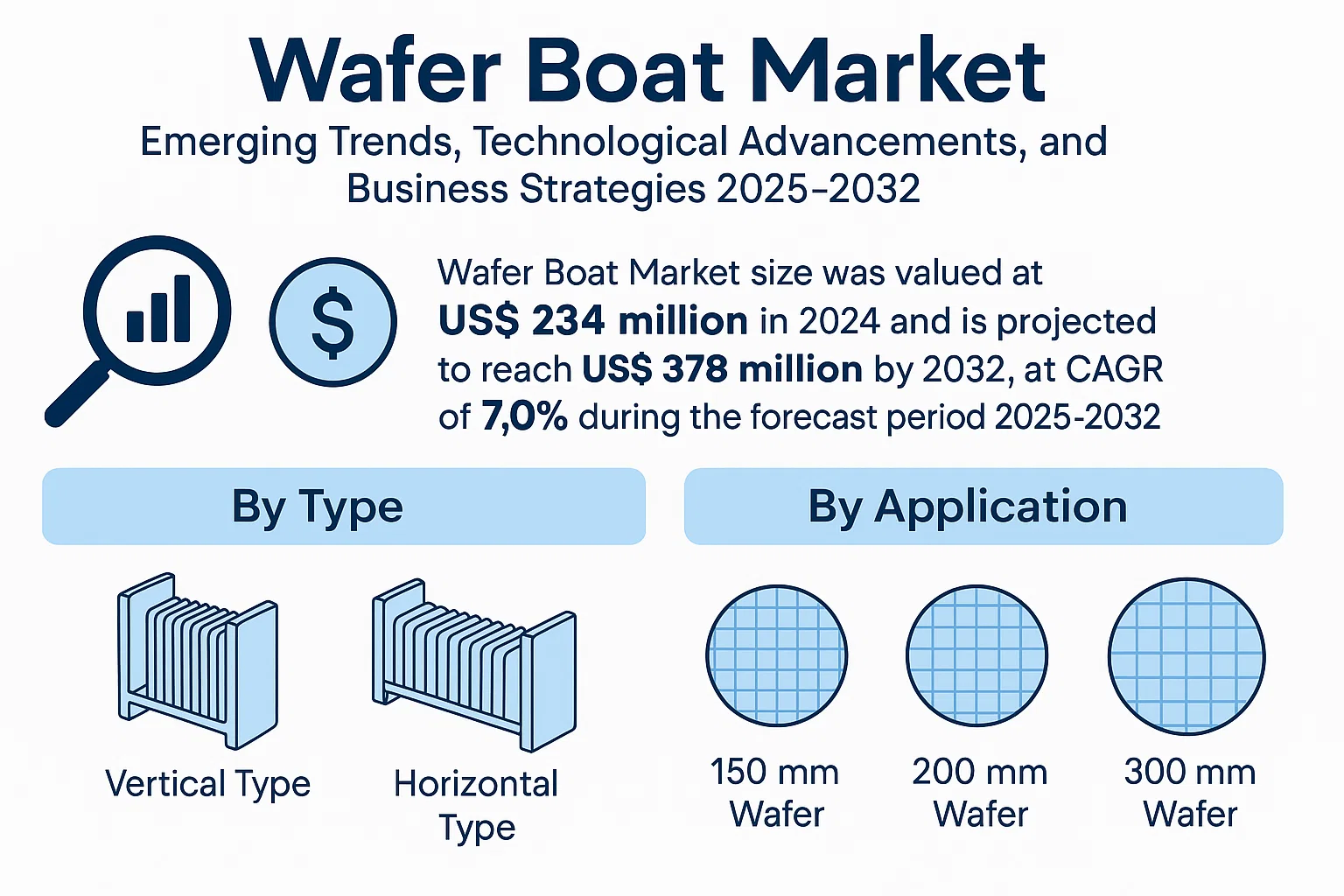
Wafer boats are precision-engineered carriers made from high-purity materials like quartz or silicon carbide. These components play an essential role in semiconductor fabrication by safely transporting wafers through high-temperature processes such as oxidation, diffusion, and chemical vapor deposition. The vertical and horizontal configurations cater to different manufacturing requirements across 150mm, 200mm, and 300mm wafer sizes.
The market growth is primarily driven by expanding semiconductor production capacities worldwide, particularly for advanced nodes below 10nm. While Asia Pacific dominates demand with over 60% market share, North America and Europe show steady growth due to reshoring initiatives in chip manufacturing. Key players like CoorsTek and Ferrotec continue to innovate with new materials and designs to meet the stringent purity and thermal stability requirements of next-generation semiconductor processes.
MARKET DYNAMICS
MARKET DRIVERS
Rapid Expansion of Semiconductor Manufacturing to Fuel Wafer Boat Demand
The global semiconductor industry is experiencing unprecedented growth, driving substantial demand for wafer boats used in thermal processing. The worldwide semiconductor market reached $580 billion in 2022, marking a 4.4% increase year-over-year despite economic headwinds. Analog chips demonstrated particularly strong performance with 20.8% growth, while sensors grew by 16.3%. With semiconductor manufacturers expanding production capacity to meet growing demand across consumer electronics, automotive, and industrial applications, wafer boat consumption is rising in parallel. Leading foundries are investing billions in new fabrication facilities, each requiring thousands of wafer boats for high-temperature processing chambers.
Transition to Larger Wafer Sizes Accelerates Equipment Upgrades
The industry’s ongoing transition from 200mm to 300mm wafer processing is creating significant replacement demand for wafer handling solutions. While mature nodes still utilize 200mm fabs for certain applications, over 70% of new capacity investments are targeting 300mm production capabilities. This technology migration necessitates entirely new sets of wafer boats designed for larger diameters, as existing 200mm equipment cannot be simply adapted. Furthermore, the introduction of advanced packaging technologies like 3D IC stacking is generating additional requirements for specialized wafer carriers capable of handling thinned wafers through multiple thermal cycles.
Material Innovation Enhances Product Performance
Advances in ceramic and quartz material science are enabling wafer boats to withstand increasingly demanding thermal cycles while minimizing particulate contamination. Manufacturers are developing proprietary material formulations that combine high-temperature stability with exceptional purity levels below 1 ppb contaminant levels. These material improvements directly translate to higher wafer yields by reducing defects caused by equipment outgassing or particle generation. The introduction of silicon carbide-coated quartz and high-purity alumina ceramics has allowed wafer boat suppliers to extend product lifetimes while meeting the stringent cleanliness requirements of sub-10nm node fabrication.
MARKET RESTRAINTS
High Capital Costs Constrain Market Penetration
The wafer boat market faces significant adoption barriers due to the substantial capital investment required for manufacturing equipment and cleanroom facilities. Establishing production capacity for high-purity ceramic wafer boats demands specialized sintering furnaces costing over $5 million per unit, along with class 100 or better cleanroom environments. These requirements create high barriers to entry that limit competition while putting upward pressure on product pricing. Smaller semiconductor manufacturers and research facilities often defer equipment upgrades due to these cost considerations, opting to extend the lifecycle of existing wafer carriers through refurbishment programs.
Supply Chain Disruptions Impact Material Availability
Critical raw material shortages continue to challenge wafer boat manufacturers, particularly for high-purity quartz and specialty ceramics. The semiconductor industry’s rapid expansion has created supply-demand imbalances for these essential materials, with lead times for quartz ingots extending beyond six months in some cases. Geopolitical factors further complicate supply chains, as certain high-purity material precursors originate from limited geographic sources. These constraints not only impact production capacity but also contribute to price volatility, making long-term cost planning difficult for both suppliers and semiconductor manufacturers.
MARKET CHALLENGES
Technical Complexity Increases with Advanced Nodes
As semiconductor manufacturing advances to 3nm and below, wafer boat designs face exponentially greater technical challenges. The transition to extreme ultraviolet (EUV) lithography and new transistor architectures requires thermal processing equipment to maintain temperature uniformity within ±0.5°C across 300mm wafers. Achieving this level of precision while preventing wafer warpage and minimizing thermal budget presents significant design hurdles. Additionally, the introduction of new substrate materials like silicon carbide and gallium nitride for power electronics creates new material compatibility concerns that wafer boat manufacturers must address through intensive R&D efforts.
Workforce Shortages Constrain Industry Growth
The specialized nature of wafer boat manufacturing presents acute staffing challenges, with demand for skilled technicians and materials scientists far outstripping supply. The industry requires workers with expertise in ceramic engineering, ultra-clean manufacturing, and semiconductor process knowledge – a rare combination that takes years to develop. Workforce shortages contribute to extended lead times and capacity constraints, with manufacturers reporting job vacancy rates exceeding 15% for critical positions. These human resource challenges are compounded by retiring experienced workers and intense competition for talent from semiconductor equipment manufacturers offering higher compensation packages.
MARKET OPPORTUNITIES
Emerging Markets Present Untapped Growth Potential
While established semiconductor manufacturing regions like Taiwan, South Korea, and the United States dominate current demand, emerging markets are rapidly developing domestic semiconductor capabilities. Government initiatives such as China’s “Big Fund” and India’s semiconductor policy are driving billions in new investments for local chip production. These developing ecosystems represent significant opportunities for wafer boat suppliers to establish early market presence through strategic partnerships with new fabs. Additionally, the geographic diversification of semiconductor manufacturing creates opportunities for localized production and service centers to better support regional customers.
Advanced Packaging Drives New Product Requirements
The rapid growth of heterogeneous integration and 3D packaging technologies is creating demand for specialized wafer handling solutions. Advanced packaging techniques such as wafer-on-wafer and chip-on-wafer bonding require carriers capable of maintaining sub-micron alignment accuracy through multiple thermal cycles. This evolving market segment presents opportunities for wafer boat manufacturers to develop innovative designs incorporating precision alignment features, low-thermal-mass structures, and compatibility with temporary bonding materials. Leaders in this space can capture significant market share as packaging becomes an increasingly critical differentiator in semiconductor performance.
WAFER BOAT MARKET TRENDS
Increasing Semiconductor Demand and Miniaturization Driving Market Growth
The global wafer boat market is experiencing significant growth, propelled by the expanding semiconductor industry and the trend toward miniaturization of electronic components. As semiconductors become increasingly integral to everything from consumer electronics to automotive systems, the need for high-precision wafer handling solutions like wafer boats has surged. The semiconductor market is expected to grow at a compound annual growth rate (CAGR) of approximately 6.5% over the next five years, directly influencing wafer boat demand. The shift toward smaller and more advanced nodes (such as 5nm and 3nm technologies) necessitates higher-quality wafer handling systems to ensure contamination-free and damage-resistant processing of delicate silicon wafers. Additionally, the rise of IoT and AI-driven devices is accelerating the need for efficient wafer-processing infrastructure, further boosting the wafer boat market.
Other Trends
Expansion of 300mm Wafer Production
The transition to 300mm wafers is reshaping the wafer boat market landscape, as these larger wafers offer better cost efficiency and higher throughput. Semiconductor manufacturers are increasingly adopting 300mm wafer fabs to optimize production capacity, with projections suggesting that 300mm wafer demand will account for over 70% of the total semiconductor market by 2030. This shift has led to a heightened requirement for durable, high-capacity wafer boats capable of handling larger wafer sizes while maintaining structural integrity under extreme thermal and chemical conditions. Emerging economies in Asia-Pacific, particularly China and Taiwan, are at the forefront of this transition, investing heavily in large-scale semiconductor fabrication facilities.
Technological Innovations and High-Performance Materials
The adoption of advanced materials such as high-purity quartz, silicon carbide, and ceramic composites is revolutionizing wafer boat manufacturing. These materials offer superior thermal stability and chemical resistance, critical for handling wafers in harsh semiconductor fabrication environments like high-temperature diffusion and etching processes. Leading wafer boat manufacturers are investing in R&D to enhance product durability, reducing particle generation—a critical factor in semiconductor yield optimization. Furthermore, automation and IoT-enabled wafer handling systems are being integrated with wafer boats to improve traceability and operational efficiency, minimizing human intervention and contamination risks. These innovations are expected to drive market growth, particularly in regions with expanding semiconductor fabrication capacities.
COMPETITIVE LANDSCAPE
Key Industry Players
Semiconductor Material Suppliers Invest in Innovation to Meet Rising Wafer Processing Demand
The global wafer boat market exhibits a moderately consolidated structure with dominant players holding significant market share. CoorsTek Inc. leads the market with an estimated 18-20% revenue share in 2024, leveraging its advanced ceramic solutions and strategic partnerships with semiconductor manufacturers. The company continues to expand its production capacity across Asia to meet growing demand.
Ferrotec Material Technologies and Integrated Materials collectively account for approximately 25% of market revenue, according to recent industry analyses. Both companies have strengthened their positions through continuous R&D investments in high-purity quartz and silicon carbide wafer boats, particularly for extreme semiconductor processing conditions.
Market competition intensifies as mid-sized players adopt vertical integration strategies. Worldex Industry recently expanded its manufacturing footprint in South Korea through a $12 million facility, while Young Shin Quartz secured multiple long-term contracts with leading foundries in Taiwan and China. This reflects the industry’s shift toward securing stable supply chains amid geopolitical uncertainties.
Emerging technologies like EUV lithography drive demand for specialized wafer handling solutions. Key players including CE-MAT and 3X Ceramic Parts are developing next-generation boats with enhanced thermal stability, targeting the 3nm and below process node requirements. Meanwhile, Chinese manufacturers like Lianyungang Shengbangda are gaining traction in domestic markets through cost-competitive offerings.
List of Key Wafer Boat Manufacturers Profiled
- CoorsTek (U.S.)
- Ferrotec Material Technologies (U.S.)
- Worldex Industry (South Korea)
- CE-MAT (Germany)
- Young Shin Quartz (South Korea)
- Feedback Technology (Taiwan)
- 3X Ceramic Parts (Japan)
- Hyman Quartz Glass (China)
- Integrated Materials (U.S.)
- Kallex (Japan)
- Lianyungang Shengbangda Quartz Products (China)
- Jinzhou Wanshida Quartz Glass (China)
Segment Analysis:
By Type
Vertical Type Segment Dominates Due to Higher Compatibility with Advanced Semiconductor Fabrication
The wafer boat market is segmented based on type into:
- Vertical Type
- Horizontal Type
By Application
300 mm Wafer Segment Leads Owing to Industry-wide Transition to Larger Wafer Sizes
The market is segmented based on application into:
- 150 mm Wafer
- 200 mm Wafer
- 300 mm Wafer
- Others
By Material
Quartz-based Wafer Boats Remain Preferred Choice for High Temperature Applications
The market is segmented based on material into:
- Quartz
- Silicon Carbide
- Ceramic
- Others
By End User Semiconductor Fab Size
Large-scale Semiconductor Fabs Account for Majority Demand
The market is segmented based on end user semiconductor fab size into:
- Megafabs (>50,000 wafer starts/month)
- Large Fabs (20,000-50,000 wafer starts/month)
- Medium Fabs (10,000-20,000 wafer starts/month)
- Small Fabs (<10,000 wafer starts/month)
Regional Analysis: Wafer Boat Market
North America
The North American wafer boat market benefits from the region’s advanced semiconductor manufacturing ecosystem, particularly in the U.S., which accounts for over 50% of global semiconductor R&D investment. The U.S. CHIPS and Science Act has allocated $52.7 billion to bolster domestic semiconductor production, directly influencing demand for wafer handling solutions. While the U.S. dominates, Canada and Mexico are emerging as strategic manufacturing hubs due to cost advantages and proximity to supply chains. Challenges include material cost inflation and competition from Asian suppliers, but the region maintains leadership in high-purity quartz and ceramic wafer boat innovations.
Europe
Europe’s market is driven by Germany and France, where precision engineering capabilities support niche wafer boat production. The region accounts for 18% of global semiconductor equipment spending, with ASML and other EUV lithography leaders necessitating ultra-clean wafer handling solutions. Strict EU regulations on material traceability (e.g., REACH compliance) add operational costs but enhance product reliability. The transition to 300mm wafer fabrication is slower than in Asia, though investments in automotive and industrial IoT semiconductors are creating steady demand. The Russia-Ukraine conflict has disrupted quartz supply chains, prompting localized sourcing strategies.
Asia-Pacific
As the semiconductor industry’s epicenter, Asia-Pacific commands 75% of global wafer boat consumption, led by China, Taiwan, South Korea, and Japan. Taiwan’s TSMC alone operates over 15 advanced fabs, creating massive demand for 300mm wafer boats. China’s semiconductor self-sufficiency push has grown domestic quartz boat production by 22% YoY, though quality disparities persist. Japan’s Shin-Etsu and Ferrotec dominate high-end synthetic quartz markets. While price competition is intense, regional players are investing in automation-compatible designs to meet the needs of next-gen fabs. Labor shortages and geopolitical tensions pose risks to just-in-time supply chains.
South America
This region remains a minor player with Brazil hosting small-scale semiconductor packaging facilities. Most wafer boats are imported from North America or Asia, with local demand growing at 3-5% annually. Argentina shows potential for quartz raw material sourcing, but economic instability limits manufacturing investments. The lack of major wafer fabs restricts market growth, though some electronics assembly plants are creating niche opportunities for 150mm and 200mm wafer handling solutions. Government incentives for tech industrialization could gradually change the landscape.
Middle East & Africa
The wafer boat market here is nascent but strategically relevant. Saudi Arabia’s $3.2 billion semiconductor initiative and Israel’s strong fabless chip design ecosystem are driving initial demand. UAE is emerging as a distribution hub for equipment suppliers targeting both regions. While no major wafer fabs exist yet, planned investments in Egypt and Morocco for automotive chips could stimulate growth. Challenges include limited technical expertise and reliance on imports, but long-term potential exists as part of global supply chain diversification efforts.
Report Scope
This market research report provides a comprehensive analysis of the Global Wafer Boat market, covering the forecast period 2025–2032. It offers detailed insights into market dynamics, technological advancements, competitive landscape, and key trends shaping the semiconductor manufacturing equipment industry.
Key focus areas of the report include:
- Market Size & Forecast: Historical data and future projections for revenue and unit shipments, with the market projected to grow at a significant CAGR during the forecast period from its 2024 valuation.
- Segmentation Analysis: Detailed breakdown by product type (Vertical and Horizontal), wafer size (150mm, 200mm, 300mm), and application areas to identify high-growth segments.
- Regional Outlook: Insights into market performance across North America, Europe, Asia-Pacific, Latin America, and Middle East & Africa, with Asia-Pacific being the dominant region.
- Competitive Landscape: Profiles of 13 key market participants including CoorsTek, Ferrotec, and Worldex Industry, covering their market share, product portfolios, and strategic initiatives.
- Technology Trends: Analysis of material innovations, thermal management solutions, and precision engineering advancements in wafer handling technologies.
- Market Drivers & Restraints: Evaluation of semiconductor industry growth, fab expansions, and technological challenges impacting wafer boat demand.
- Stakeholder Analysis: Strategic insights for semiconductor equipment manufacturers, material suppliers, and investors in the wafer processing value chain.
The research methodology combines primary interviews with wafer boat manufacturers and secondary data analysis from industry reports to ensure data accuracy and reliability.
FREQUENTLY ASKED QUESTIONS:
What is the current market size of Global Wafer Boat Market?
-> Wafer Boat Market size was valued at US$ 234 million in 2024 and is projected to reach US$ 378 million by 2032, at a CAGR of 7.0%.
Which key companies operate in Global Wafer Boat Market?
-> Key players include CoorsTek, Ferrotec Material Technologies, Worldex Industry, CE-MAT, and Young Shin Quartz, among others.
What are the key growth drivers?
-> Key growth drivers include semiconductor industry expansion, increasing wafer sizes, and advanced node manufacturing requirements.
Which region dominates the market?
-> Asia-Pacific dominates the market due to concentrated semiconductor manufacturing activities in China, Taiwan, South Korea and Japan.
What are the emerging trends?
-> Emerging trends include high-purity quartz materials, automated wafer handling solutions, and thermal-resistant coating technologies.

Get Sample Report PDF for Exclusive Insights
Report Sample Includes
- Table of Contents
- List of Tables & Figures
- Charts, Research Methodology, and more...