MARKET INSIGHTS
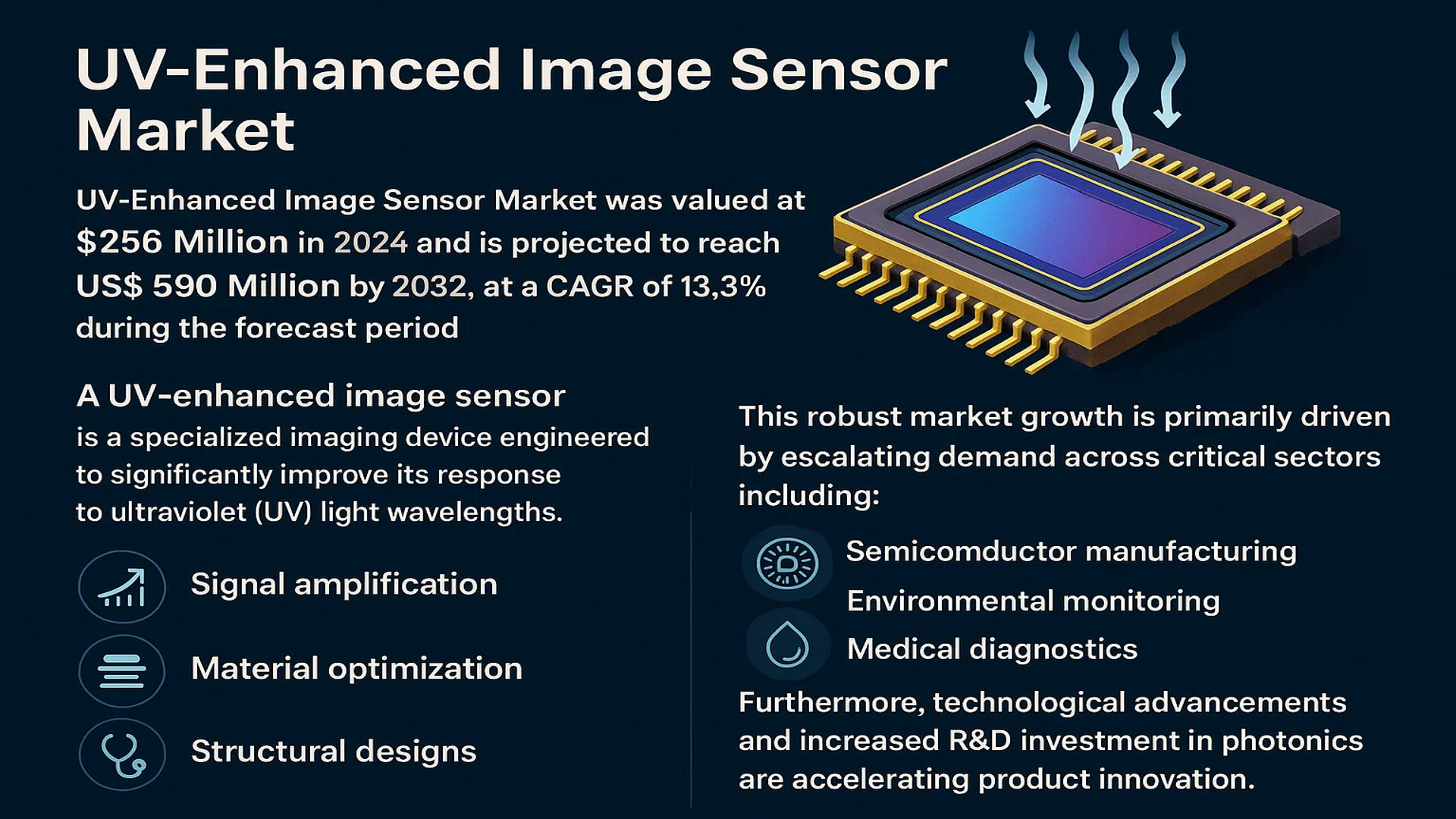
The global UV-Enhanced Image Sensor Market was valued at 256 million in 2024 and is projected to reach US$ 590 million by 2032, at a CAGR of 13.3% during the forecast period.
A UV-enhanced image sensor is a specialized imaging device engineered to significantly improve its response to ultraviolet (UV) light wavelengths. Unlike conventional sensors, these devices employ advanced techniques such as signal amplification, material optimization, and unique structural designs to achieve superior detection sensitivity, enhanced signal-to-noise ratio, and greater environmental adaptability within the UV spectrum.
This robust market growth is primarily driven by escalating demand across critical sectors including semiconductor manufacturing, environmental monitoring, and medical diagnostics. Furthermore, technological advancements and increased R&D investment in photonics are accelerating product innovation. The market is highly concentrated, with key players like Sony Semiconductor Solutions Group, Hamamatsu Photonics, ams OSRAM, and Teledyne collectively holding a significant revenue share. Recent developments, such as the introduction of higher-resolution sensors for industrial inspection, continue to fuel expansion and adoption.
MARKET DYNAMICS
MARKET DRIVERS
Expanding Applications in Semiconductor Manufacturing to Drive Market Growth
The semiconductor industry’s relentless pursuit of miniaturization and precision has created substantial demand for UV-enhanced image sensors. These sensors enable critical inspection processes for wafers and photomasks by detecting microscopic defects and contaminants that are invisible under visible light. The global semiconductor manufacturing equipment market, valued at over $100 billion annually, increasingly relies on advanced metrology and inspection systems incorporating UV imaging technology. With the transition to 3nm and smaller process nodes, the requirement for defect detection sensitivity below 10nm has become essential, driving adoption of UV-enhanced sensors capable of resolving features at these scales. Major semiconductor equipment manufacturers are integrating these sensors into their latest inspection systems to maintain yield rates exceeding 90% in advanced fabrication facilities.
Growing Environmental Monitoring Requirements to Accelerate Adoption
Environmental monitoring applications represent a significant growth driver for UV-enhanced image sensors, particularly in air and water quality assessment. These sensors enable detection of specific pollutants and biological agents through their unique UV fluorescence signatures. The global environmental monitoring market is projected to exceed $30 billion by 2028, with UV-based detection systems capturing an increasing share. Governments worldwide are implementing stricter environmental regulations requiring continuous monitoring of industrial emissions and water treatment outputs. UV-enhanced sensors provide the sensitivity needed to detect trace levels of contaminants at parts-per-billion concentrations, making them indispensable for compliance monitoring. The ability to perform real-time, non-contact measurements in harsh industrial environments further enhances their value proposition for environmental applications.
Advancements in Medical Diagnostics to Fuel Market Expansion
Medical diagnostics represents a rapidly growing application area for UV-enhanced image sensors, particularly in fluorescence-based imaging and spectroscopy. The global medical imaging market, valued at approximately $40 billion, is incorporating UV-enhanced technologies for improved disease detection and research capabilities. These sensors enable detection of fluorescent biomarkers and probes used in cancer diagnostics, genetic analysis, and drug discovery applications. The increasing prevalence of chronic diseases worldwide, coupled with growing investment in precision medicine, is driving demand for advanced diagnostic tools utilizing UV imaging. Research institutions and pharmaceutical companies are adopting these sensors for high-throughput screening and molecular imaging, where their enhanced sensitivity enables detection of low-concentration biomarkers that conventional sensors might miss.
MARKET CHALLENGES
High Development and Manufacturing Costs to Constrain Market Penetration
The specialized materials and manufacturing processes required for UV-enhanced image sensors present significant cost challenges. Production of these sensors involves expensive semiconductor-grade silicon and specialized coating materials that can increase manufacturing costs by 40-60% compared to conventional image sensors. The development of UV-optimized pixel structures requires cleanroom facilities meeting Class 100 standards or better, with investment in specialized deposition and etching equipment costing millions of dollars per fabrication line. These high capital and operational expenses create barriers to entry for new market participants and limit production scalability. Additionally, the yield rates for UV-enhanced sensors typically range between 65-75% compared to 85-90% for standard sensors, further increasing per-unit costs and challenging mass-market adoption.
Other Challenges
Technical Complexity in System Integration
Integrating UV-enhanced sensors into complete imaging systems presents substantial technical challenges. These sensors require specialized optical components, including UV-transparent lenses and filters that can maintain performance under prolonged UV exposure. System designers must address issues of UV-induced degradation of optical materials and develop calibration methods that account for sensor response variations across the UV spectrum. The need for customized readout electronics and signal processing algorithms adds further complexity, requiring multidisciplinary expertise in optics, semiconductor physics, and image processing.
Limited Standardization Across Applications
The absence of industry-wide standards for UV-enhanced image sensors creates interoperability challenges and increases development costs. Different applications require varying performance specifications regarding quantum efficiency, dark current, and readout noise, leading to fragmentation in sensor designs and manufacturing processes. This lack of standardization complicates the development of universal testing methodologies and performance benchmarks, making it difficult for end-users to compare products across manufacturers and select appropriate solutions for their specific applications.
MARKET RESTRAINTS
Material Limitations and Performance Trade-offs to Restrict Market Growth
UV-enhanced image sensors face fundamental material limitations that restrict their performance and application scope. Conventional silicon-based sensors exhibit rapidly decreasing quantum efficiency below 400nm, typically falling below 10% in the UV-C band (200-280nm). While specialized coatings and material modifications can improve UV response, these enhancements often come at the cost of reduced performance in visible wavelengths or increased dark current. The trade-off between UV sensitivity and overall sensor performance creates design constraints that limit adoption in applications requiring broadband imaging capabilities. Additionally, UV-induced damage to sensor materials can reduce operational lifetime, particularly in high-flux applications such as semiconductor inspection or scientific research, where sensors may be exposed to intense UV radiation for extended periods.
Supply Chain Constraints for Specialized Materials to Impede Production Scaling
The production of UV-enhanced image sensors relies on specialized materials with limited global supply chains and high cost structures. Materials such as high-purity quartz for optical components, specialized anti-reflection coatings, and UV-transparent packaging materials face supply constraints and price volatility. The global semiconductor materials market, while growing at approximately 6% annually, experiences periodic shortages of these specialized components, particularly those requiring custom manufacturing processes. These supply chain challenges are exacerbated by the concentration of manufacturing capabilities among a limited number of suppliers, creating dependency risks for sensor manufacturers. The lead times for certain critical materials can extend to 6-9 months, complicating production planning and limiting the ability to respond quickly to changes in market demand.
Technical Expertise Shortage to Slow Innovation and Adoption
The specialized nature of UV-enhanced image sensor technology creates a significant barrier in terms of required technical expertise. The field requires knowledge spanning ultraviolet optics, semiconductor physics, materials science, and image processing algorithms. The global shortage of engineers and scientists with experience in UV imaging technology is estimated to affect over 30% of companies operating in this space. This expertise gap slows innovation cycles and impedes the development of new applications. Furthermore, the complexity of integrating these sensors into complete systems requires multidisciplinary teams that are difficult to assemble and retain, particularly given the competition for talent from adjacent technology sectors offering higher compensation packages and more established career paths.
MARKET OPPORTUNITIES
Emerging Applications in Life Sciences and Healthcare to Create New Growth Avenues
The life sciences and healthcare sectors present substantial growth opportunities for UV-enhanced image sensors, particularly in fluorescence microscopy and DNA sequencing applications. The global life sciences instrumentation market, exceeding $60 billion annually, is increasingly adopting UV imaging for advanced research techniques. These sensors enable detection of low-intensity fluorescence signals from biological samples, supporting research in genomics, proteomics, and drug discovery. The growing investment in personalized medicine and molecular diagnostics is driving demand for imaging systems capable of detecting UV-excited fluorophores with high sensitivity and quantitative accuracy. Additionally, the expansion of point-of-care diagnostics and portable medical devices creates opportunities for miniaturized UV imaging systems that can perform rapid analyses in clinical settings.
Advancements in Automotive and Industrial Safety Systems to Drive Future Demand
UV-enhanced image sensors are finding new applications in automotive and industrial safety systems, particularly for flame and arc detection. The global industrial safety market, projected to reach $8 billion by 2028, incorporates UV imaging for early detection of electrical arcs and combustion events in high-risk environments. These sensors can detect UV emissions from electrical faults and fires before they become visible to conventional sensors or human operators, enabling faster response times and reducing damage. In the automotive sector, UV sensors are being integrated into battery management systems for electric vehicles to detect early signs of thermal runaway and electrical faults. The move toward autonomous vehicles and advanced driver assistance systems creates additional opportunities for multi-spectral imaging systems incorporating UV sensing capabilities.
Development of Multi-spectral and Hyperspectral Imaging Systems to Expand Addressable Market
The integration of UV-enhanced sensors into multi-spectral and hyperspectral imaging systems represents a significant growth opportunity across multiple industries. These advanced imaging systems combine UV, visible, and infrared sensing capabilities to provide comprehensive material analysis and identification. The global hyperspectral imaging market is growing at over 12% annually, with applications expanding from traditional remote sensing to agriculture, food safety, and pharmaceutical quality control. UV-enhanced sensors add critical capability for detecting and characterizing materials based on their UV fluorescence and absorption properties. The development of compact, cost-effective multi-spectral systems is making this technology accessible to smaller enterprises and new application areas, potentially expanding the addressable market by 25-30% over the next five years.
UV-ENHANCED IMAGE SENSOR MARKET TRENDS
Advancements in Semiconductor Fabrication and Inspection to Emerge as a Trend in the Market
The relentless drive towards smaller semiconductor nodes, particularly below 10nm, has created an unprecedented demand for highly sophisticated inspection and metrology tools. UV-enhanced image sensors, with their superior sensitivity to shorter wavelengths, are becoming indispensable in this domain because they enable the detection of sub-micron defects and contaminants that are invisible to standard visible light sensors. This capability is critical for maintaining high yields in advanced fabrication processes. The global semiconductor equipment market, a key driver for these sensors, is projected to exceed $140 billion by 2025, underscoring the massive scale of this demand. Furthermore, the integration of these sensors with artificial intelligence and machine learning for automated defect classification and process control is significantly enhancing their value proposition, moving beyond simple detection to predictive analytics and process optimization.
Other Trends
Expansion in Environmental and Scientific Monitoring
Beyond industrial applications, there is a growing utilization of UV-enhanced image sensors in environmental monitoring and scientific research. These sensors are pivotal in instruments designed for ozone layer monitoring, flame detection, and UV index measurement, providing critical data for climate science and public safety. The precision required in spectroscopic applications for chemical analysis and material characterization also benefits greatly from the high signal-to-noise ratio offered by these specialized sensors. This trend is supported by increased global investment in climate tech and scientific R&D, which is fostering innovation and creating new, high-value applications for UV imaging technology across various research institutions and environmental agencies.
Medical and Life Sciences Diagnostic Applications
The medical and life sciences sector represents a significant growth frontier for UV-enhanced image sensors, particularly in fluorescence-based diagnostic techniques. These sensors are essential components in equipment used for DNA sequencing, gel documentation, and fluorescence microscopy, where their ability to detect low-intensity UV-induced fluorescence signals with high clarity is paramount. The global genomics market, which heavily relies on such technologies, is on a robust growth trajectory and is expected to surpass $54 billion by 2028. This expansion is directly fueling demand for more sensitive and reliable imaging components. Recent technological improvements have focused on increasing quantum efficiency in the UV spectrum while simultaneously reducing dark current, thereby enhancing the accuracy of diagnostic results and enabling earlier disease detection and more precise research outcomes.
COMPETITIVE LANDSCAPE
Key Industry Players
Leading Manufacturers Drive Innovation Through Technological Advancements and Strategic Expansions
The global UV-enhanced image sensor market exhibits a moderately consolidated structure, dominated by several established technology giants alongside specialized photonics companies. Sony Semiconductor Solutions Group maintains a formidable position, leveraging its extensive semiconductor manufacturing expertise and global distribution network. The company’s leadership stems from its continuous investment in CMOS sensor technology and ability to scale production for diverse applications ranging from consumer electronics to industrial instrumentation.
Hamamatsu Photonics and ams OSRAM represent another tier of significant market participants, collectively holding substantial market share. Hamamatsu’s strength lies in its deep-rooted expertise in photonic technologies and strong presence in scientific and research applications, while ams OSRAM benefits from its integrated approach combining sensor technology with advanced illumination solutions. Both companies have demonstrated consistent growth through specialized product development and strategic partnerships with research institutions and industrial clients.
Market competition intensifies as companies pursue technological differentiation through material science innovations and architectural improvements. Recent industry developments include the introduction of back-illuminated UV sensors with enhanced quantum efficiency and the development of multispectral sensors capable of simultaneous UV and visible light detection. These advancements address growing demand across semiconductor manufacturing, where UV sensors enable precise lithography control, and environmental monitoring applications, where they facilitate accurate detection of atmospheric pollutants and ozone layer measurements.
Teledyne Technologies has emerged as a particularly aggressive competitor, strengthening its market position through strategic acquisitions and focused R&D investments. The company’s 2023 acquisition of a specialized UV sensor manufacturer expanded its capabilities in fluorescence-based detection systems, positioning it strongly for medical and life science applications. Similarly, Sony’s ongoing development of stacked CMOS sensors with improved UV sensitivity demonstrates how market leaders continuously refresh their product portfolios to maintain technological leadership.
The competitive environment continues to evolve as established players face challenges from specialized startups focusing on niche applications. While large corporations dominate high-volume markets, smaller innovators increasingly capture value in specialized segments such as biomedical imaging and forensic analysis. This dynamic ensures ongoing innovation across the market spectrum, driving performance improvements and cost reductions that benefit end-users across industries.
List of Key UV-Enhanced Image Sensor Companies Profiled
- Sony Semiconductor Solutions Group (Japan)
- Hamamatsu Photonics K.K. (Japan)
- ams OSRAM AG (Austria)
- Teledyne Technologies Incorporated (U.S.)
- ON Semiconductor Corporation (U.S.)
- STMicroelectronics N.V. (Switzerland)
- Panasonic Corporation (Japan)
- Canon Inc. (Japan)
- OmniVision Technologies, Inc. (U.S.)
Segment Analysis:
By Type
Fluorescence Conversion Type Segment Leads the Market Due to Superior Sensitivity and Broader Application Range
The market is segmented based on type into:
- Fluorescence Conversion Type
- Subtypes: Silicon-based, Gallium Nitride (GaN)-based, and others
- Electron Multiplication Type
- Subtypes: Back-Illuminated, Front-Illuminated, and others
- Others
- Subtypes: Hybrid sensors and emerging material-based sensors
By Application
Semiconductor Segment Dominates Owing to Critical Use in Lithography and Wafer Inspection Processes
The market is segmented based on application into:
- Semiconductor
- Sub-applications: Lithography alignment, defect inspection, and metrology
- Environmental Monitoring
- Sub-applications: Ozone layer monitoring, UV index measurement, and pollution tracking
- Research
- Sub-applications: Astronomical observations, material science, and chemical analysis
- Medical
- Sub-applications: Dermatology imaging, sterilization validation, and fluorescence-guided surgery
- Others
- Sub-applications: Forensic analysis and art restoration
By End User
Industrial Manufacturing Sector Holds Largest Share Driven by High-Volume Adoption in Quality Control
The market is segmented based on end user into:
- Industrial Manufacturing
- Sub-segments: Semiconductor fabrication plants and electronics assembly
- Healthcare & Life Sciences
- Sub-segments: Hospitals, research laboratories, and diagnostic centers
- Government & Defense
- Sub-segments: Space agencies, environmental protection agencies, and military
- Academic & Research Institutions
- Sub-segments: Universities and private research organizations
- Others
- Sub-segments: Commercial and consumer applications
Regional Analysis: UV-Enhanced Image Sensor Market
Asia-Pacific
The Asia-Pacific region is the dominant force in the global UV-enhanced image sensor market, driven primarily by massive semiconductor manufacturing hubs and significant government investments in R&D. China, Japan, and South Korea are the key contributors, with China alone projected to represent a substantial portion of the global market value by 2032. The region’s strength stems from its integrated electronics supply chain and the proliferation of applications in industrial automation, environmental monitoring, and biomedical research. While cost-competitive manufacturing is a hallmark, there is a clear and accelerating trend toward developing higher-sensitivity, next-generation sensors to maintain technological leadership. The presence of major global players like Sony Semiconductor Solutions Group and Hamamatsu Photonics, coupled with a thriving ecosystem of specialized suppliers, ensures continuous innovation and production scalability to meet both regional and international demand.
North America
North America, particularly the United States, is a critical innovation center for advanced UV-enhanced image sensor technologies. The market is propelled by high-value applications in defense, aerospace, and life sciences, where performance and reliability are paramount over cost. Substantial funding from agencies like the Department of Defense and the National Institutes of Health fuels research into cutting-edge sensor designs, including backside-illuminated (BSI) and electron multiplication types for low-light scientific imaging. Leading companies such as Teledyne Technologies are headquartered here, focusing on developing sensors for extreme environments and specialized instrumentation. While manufacturing volume may be lower than in Asia, the region excels in creating high-margin, proprietary technologies that set global performance benchmarks and are exported worldwide.
Europe
Europe maintains a strong, technologically advanced market characterized by a focus on precision engineering, quality, and adherence to stringent regulatory standards. Germany, the UK, and France are the core markets, with demand driven by the automotive sector (for flame detection and gas analysis), sophisticated medical imaging equipment, and environmental monitoring systems complying with EU directives. Companies like ams OSRAM are key innovators, often collaborating with research institutions and industrial partners to develop sensors for specific high-end applications. The market’s growth is steady, supported by a robust industrial base that values long-term reliability and integration into complex systems, though it faces cost pressures from higher-volume Asian manufacturing.
South America
The South American market for UV-enhanced image sensors is nascent but shows potential for gradual growth. Current adoption is primarily limited to academic and research institutions and specific industrial applications, such as mineralogy and food safety inspection in countries like Brazil and Argentina. The market is constrained by economic volatility, which limits large-scale capital investment in advanced sensor technology, and a relatively underdeveloped local manufacturing and R&D ecosystem. Most demand is met through imports from North American, European, or Asian suppliers. However, increasing awareness of environmental monitoring and gradual industrial modernization present long-term opportunities for market expansion, albeit from a small base.
Middle East & Africa
This region represents an emerging market with growth potential tied to specific industrial and governmental initiatives. Key applications are found in the oil and gas sector for flare monitoring and leak detection, as well as in security and defense projects in nations like Israel, Turkey, and Saudi Arabia. The UAE is also investing in technological infrastructure that could incorporate advanced sensing for environmental and smart city projects. However, the overall market size remains small due to limited local technological development and a reliance on international suppliers for high-tech components. Progress is often linked to large-scale government-funded projects rather than organic, broad-based industrial demand.
Report Scope
This market research report provides a comprehensive analysis of the global and regional UV-Enhanced Image Sensor markets, covering the forecast period 2025–2032. It offers detailed insights into market dynamics, technological advancements, competitive landscape, and key trends shaping the industry.
Key focus areas of the report include:
- Market Size & Forecast: Historical data and future projections for revenue, unit shipments, and market value across major regions and segments.
- Segmentation Analysis: Detailed breakdown by product type, technology, application, and end-user industry to identify high-growth segments and investment opportunities.
- Regional Outlook: Insights into market performance across North America, Europe, Asia-Pacific, Latin America, and the Middle East & Africa, including country-level analysis where relevant.
- Competitive Landscape: Profiles of leading market participants, including their product offerings, R&D focus, manufacturing capacity, pricing strategies, and recent developments such as mergers, acquisitions, and partnerships.
- Technology Trends & Innovation: Assessment of emerging technologies, integration of AI/IoT, semiconductor design trends, fabrication techniques, and evolving industry standards.
- Market Drivers & Restraints: Evaluation of factors driving market growth along with challenges, supply chain constraints, regulatory issues, and market-entry barriers.
- Stakeholder Analysis: Insights for component suppliers, OEMs, system integrators, investors, and policymakers regarding the evolving ecosystem and strategic opportunities.
Primary and secondary research methods are employed, including interviews with industry experts, data from verified sources, and real-time market intelligence to ensure the accuracy and reliability of the insights presented.
FREQUENTLY ASKED QUESTIONS:
What is the current market size of Global UV-Enhanced Image Sensor Market?
-> UV-Enhanced Image Sensor Market was valued at 256 million in 2024 and is projected to reach US$ 590 million by 2032, at a CAGR of 13.3% during the forecast period.
Which key companies operate in Global UV-Enhanced Image Sensor Market?
-> Key players include Sony Semiconductor Solutions Group, Hamamatsu Photonics, ams OSRAM, and Teledyne, among others.
What are the key growth drivers?
-> Key growth drivers include increasing demand in semiconductor manufacturing, advancements in environmental monitoring technologies, and growing applications in medical and research fields.
Which region dominates the market?
-> Asia-Pacific is the fastest-growing region, driven by significant manufacturing and technological adoption in countries like China and Japan, while North America remains a key market due to advanced research and development activities.
What are the emerging trends?
-> Emerging trends include integration of AI for enhanced image processing, development of more sensitive and durable sensors, and expansion into new application areas such as biotechnology and aerospace.

Get Sample Report PDF for Exclusive Insights
Report Sample Includes
- Table of Contents
- List of Tables & Figures
- Charts, Research Methodology, and more...


