
Key Statistics
Key Takeaways
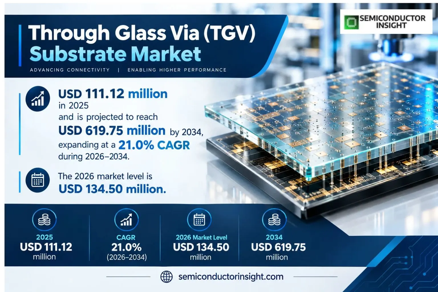
- Market size: The market is valued at USD 111.12 million in 2025 and is projected to reach USD 619.75 million by 2034, representing a 21.0% CAGR during 2026–2034.
- 300 mm wafers are the leading type, reflecting the shift toward larger formats that improve throughput for advanced packaging and RF applications.
- Consumer electronics remains the largest application, while AI packaging, automotive electronics and co-packaged optics are expanding the strategic opportunity.
- Japan is the largest individual country market in the reference analysis, followed by North America and Europe, while broader Asia Pacific provides the strongest growth profile.
- High-volume manufacturing readiness is the central competitive issue, with via quality, crack control, metallization yield and panel-scale process integration determining commercialization speed.
Through Glass Via (TGV) Substrate Market Overview
Through glass via TGV substrate market is valued at USD 111.12 million in 2025 and is projected to reach USD 619.75 million by 2034, expanding at a 21.0% CAGR during 2026–2034. The 2026 market level is USD 134.50 million. Asia Pacific leads through Japan, Korea and the broader electronics-packaging ecosystem. TGV substrates are gaining strategic importance because glass combines low electrical loss, adjustable thermal expansion and fine through-via capability for RF, MEMS, advanced packaging and emerging AI interposer applications.
Through Glass Via substrates use precision vias formed through glass and metallized to create vertical electrical interconnects. Glass offers low dielectric loss at high frequencies, high stiffness, smooth surfaces and adjustable coefficient of thermal expansion. These properties make TGV attractive for RF front ends, interposers, MEMS, sensors and advanced package structures where signal integrity, dimensional stability and fine-pitch routing are important.
Commercial manufacturing requires via formation, cleaning, seed-layer deposition, copper plating, planarization and inspection without cracking the glass or leaving voids in the metal fill. Corning offers wafer and panel-format TGV glass, while LPKF’s LIDE process focuses on crack-free high-precision via formation suitable for scale-up. Metallization and defect inspection remain critical process-development areas as customers move from prototypes toward high-volume manufacturing.
TGV competes with silicon interposers and organic substrates, so adoption depends on total package economics rather than material properties alone. Glass can reduce high-frequency loss and potentially support larger panel formats, but it requires specialized handling and via-processing expertise. Suppliers that can provide qualified materials together with scalable via and metallization processes are best positioned to win advanced packaging programs.
Segment Analysis: By Type
By type, the market is segmented into 300 mm, 200 mm and ≤150 mm wafers. The 300 mm segment leads because larger substrates improve process throughput and align with advanced semiconductor manufacturing infrastructure. Smaller diameters remain relevant for specialty RF, MEMS, sensor and development applications where flexible processing or lower absolute substrate cost matters more than maximum manufacturing efficiency.
| Type | Commercial role |
|---|---|
| 300 mm Wafer | Leading commercial format for advanced packaging and higher-throughput manufacturing. |
| 200 mm Wafer | Established format for specialty packaging, RF and development programs. |
| ≤150 mm Wafer | Research, MEMS and lower-volume specialty applications. |
Additional Segmentation: By Glass Format
Glass can be processed in wafer or panel format. Wafer formats integrate more easily with existing semiconductor tools, while panel formats offer a path to lower cost per unit area and higher package throughput if handling, alignment and metallization yield are controlled. The ability to scale TGV beyond conventional wafer sizes is one of the technology’s most important economic differentiators.
| Glass Format | Demand characteristics |
|---|---|
| Wafer Format | Compatible with semiconductor process tools and precision wafer-level packaging. |
| Panel Format | Larger-area processing aimed at higher throughput and lower cost per package. |
Segment Analysis: By Application
By application, consumer electronics is the largest current segment, followed by automotive and other specialized uses. RF filters, sensors and compact modules benefit from glass electrical properties, while advanced packaging for AI and high-performance computing is emerging as a higher-value opportunity. Automotive adoption is driven by radar, sensing and increasingly complex electronic modules.
| Application | Demand characteristics |
|---|---|
| Consumer Electronics | RF modules, compact sensors and advanced packaging for high-density devices. |
| Automobile Industry | Radar, sensing, power and high-reliability electronics. |
| Others | MEMS, photonics, aerospace, medical and advanced computing packages. |
Additional Segmentation: By Integration Use
Integration use separates RF interposers, MEMS and sensors, advanced packaging with chiplets, and co-packaged optics. RF applications value low dielectric loss, MEMS and sensors use dimensional stability and fine vias, while AI packaging requires high I/O density and large substrate formats. Co-packaged optics adds stringent requirements for optical alignment and low-loss electrical interconnect around photonic engines.
| Integration Use | Commercial relevance |
|---|---|
| RF Interposer | Low-loss routing and passive integration for high-frequency modules. |
| MEMS & Sensors | Compact vertical interconnect and stable glass platforms for sensing devices. |
| Advanced Packaging & Chiplets | High-density interposer and redistribution structures for heterogeneous integration. |
| Co-Packaged Optics | Glass routing and integration around optical engines and high-speed switch packages. |
Regional Analysis
Japan is the largest individual country market in the reference analysis, while Asia Pacific as a broader region provides the strongest growth environment. North America and Europe remain major markets through semiconductor packaging R&D and high-value RF or advanced packaging applications. Other regions are much smaller and mostly participate through downstream electronics manufacturing.
Why does regional demand differ across the Through Glass Via (TGV) Substrate market?
Regional advantage depends on materials expertise, packaging equipment, semiconductor customers and high-volume manufacturing know-how. Japan and Korea have strong glass and packaging ecosystems, North America contributes advanced package architecture and RF demand, and Europe provides precision equipment and research. The market remains highly concentrated among a limited number of companies with proprietary glass-processing capability.
| Region | Position | Demand profile | Supplier-selection factor |
|---|---|---|---|
| Asia Pacific | Largest / fastest | Packaging, RF, electronics | Glass and packaging ecosystem |
| North America | Major | Advanced packaging, RF | Architecture and R&D leadership |
| Europe | Major | Equipment, RF, research | Precision processing |
| South America | Emerging | Downstream electronics | Imported technology |
| Middle East & Africa | Emerging | Research and electronics | Project-led demand |
Competitive Landscape
Corning, LPKF, KISO WAVE, Samtec and Xiamen Sky Semiconductor are among the leading companies identified in the reference market. Competitive advantage depends on glass composition, via formation quality, metallization compatibility, defect density and the ability to support larger wafer or panel formats without compromising yield. For commercial decisions in the Through Glass Via (TGV) Substrate market, buyers also weigh qualification evidence, integration effort, operating reliability, lifecycle support, supply continuity and measurable system-level value rather than a single specification.
Corning differentiates through specialty glass materials with adjustable CTE and precision TGV capability, while LPKF provides laser-induced deep etching technology designed for crack-free high-volume via formation. Other suppliers compete through specialized interposer design, metallization and regional manufacturing relationships. For commercial decisions in the Through Glass Via (TGV) Substrate market, buyers also weigh qualification evidence, integration effort, operating reliability, lifecycle support, supply continuity and measurable system-level value rather than a single specification.
The market is concentrated because process know-how is difficult to replicate. A substrate supplier must control not only hole geometry but also downstream metallization, warpage, surface quality and reliability. Partnerships between glass, equipment and metallization providers are therefore increasingly important for scaling from R&D into volume production. For commercial decisions in the Through Glass Via (TGV) Substrate market, buyers also weigh qualification evidence, integration effort, operating reliability, lifecycle support, supply continuity and measurable system-level value rather than a single specification.
| Competitive tier | Representative companies | Primary differentiation |
|---|---|---|
| Glass material leaders | Corning, specialty glass manufacturers | Glass composition, CTE control and precision substrate supply. |
| TGV process-equipment leaders | LPKF and specialized laser-processing companies | High-precision via formation and manufacturing scale-up. |
| Packaging / substrate specialists | KISO WAVE, Samtec, Xiamen Sky Semiconductor | Interposer, metallization and application-specific TGV solutions. |
Key companies profiled
Corning, LPKF, KISO WAVE Co., Samtec, Xiamen Sky Semiconductor and other specialty glass and advanced packaging companies are included in the competitive scope. The top tier is relatively concentrated because high-volume TGV requires proprietary process integration across glass, laser structuring, metallization and reliability testing. For commercial decisions in the Through Glass Via (TGV) Substrate market, buyers also weigh qualification evidence, integration effort, operating reliability, lifecycle support, supply continuity and measurable system-level value rather than a single specification.
Production Capacity Analysis
TGV capacity depends on glass-sheet production, via drilling or laser modification, chemical processing, seed deposition, copper filling, planarization and inspection. The challenge is not simply creating holes: high-volume lines must achieve low crack rates, consistent via geometry and void-free metallization across large substrates. For commercial decisions in the Through Glass Via (TGV) Substrate market, buyers also weigh qualification evidence, integration effort, operating reliability, lifecycle support, supply continuity and measurable system-level value rather than a single specification.
Scale-up increasingly favors panel-compatible processes and automated inspection. LPKF has emphasized that HVM success requires process integration rather than isolated via formation. Corning’s ability to supply glass in both wafer and panel formats creates flexibility for customers optimizing package size and cost. For commercial decisions in the Through Glass Via (TGV) Substrate market, buyers also weigh qualification evidence, integration effort, operating reliability, lifecycle support, supply continuity and measurable system-level value rather than a single specification.
Market Dynamics
The market is driven by advanced packaging, 5G/RF demand, AI chiplets, MEMS and package miniaturization. Growth is restrained by manufacturing complexity, metallization yield and the cost of specialized equipment. Panel processing, AI package interposers and co-packaged optics provide the strongest opportunities for step-change growth. For commercial decisions in the Through Glass Via (TGV) Substrate market, buyers also weigh qualification evidence, integration effort, operating reliability, lifecycle support, supply continuity and measurable system-level value rather than a single specification.
Market Drivers
| Driver | Impact | Commercial mechanism |
|---|---|---|
| Advanced packaging | High | Chiplets and heterogeneous integration need dense low-loss interconnect. |
| 5G and RF | High | Glass offers low electrical loss at high frequency. |
| Panel-level manufacturing | Medium-High | Larger substrates can lower cost per package. |
| MEMS and sensors | Medium | Glass provides dimensional stability and transparent or insulating properties. |
Advanced packaging
TGV substrates can provide fine vertical connections and stable glass interposers for complex multi-die packages. AI and high-performance computing increase the need for large substrate area and high I/O density. For commercial decisions in the Through Glass Via (TGV) Substrate market, buyers also weigh qualification evidence, integration effort, operating reliability, lifecycle support, supply continuity and measurable system-level value rather than a single specification.
5G and RF
RF filters, antennas and front-end modules benefit from low dielectric loss and the ability to form passive structures in glass. These properties create a durable application base beyond leading-edge compute packaging. For commercial decisions in the Through Glass Via (TGV) Substrate market, buyers also weigh qualification evidence, integration effort, operating reliability, lifecycle support, supply continuity and measurable system-level value rather than a single specification.
Panel-level manufacturing
Glass can be produced in panel formats, potentially increasing throughput compared with wafer-limited approaches. Commercial value depends on maintaining alignment, via quality and metallization yield across the larger area. For commercial decisions in the Through Glass Via (TGV) Substrate market, buyers also weigh qualification evidence, integration effort, operating reliability, lifecycle support, supply continuity and measurable system-level value rather than a single specification.
MEMS and sensors
MEMS, sensor and photonic packages can use glass to route electrical signals while maintaining mechanical stability and low parasitic loss. TGV enables compact three-dimensional integration. For commercial decisions in the Through Glass Via (TGV) Substrate market, buyers also weigh qualification evidence, integration effort, operating reliability, lifecycle support, supply continuity and measurable system-level value rather than a single specification.
Market Restraints
| Restraint | Impact | Commercial consequence |
|---|---|---|
| Via and metallization yield | High | Cracks, voids and poor adhesion can destroy package reliability. |
| Manufacturing cost | Medium-High | Specialized laser, plating and handling equipment raises capital intensity. |
| Glass handling | Medium | Thin glass can be fragile during high-throughput processing. |
| Ecosystem maturity | Medium | Volume supply chains are less mature than conventional substrates. |
Via and metallization yield
High aspect-ratio vias require precise formation and complete metal fill. Small defects can become yield loss after significant downstream processing, making inspection and process control essential. For commercial decisions in the Through Glass Via (TGV) Substrate market, buyers also weigh qualification evidence, integration effort, operating reliability, lifecycle support, supply continuity and measurable system-level value rather than a single specification.
Manufacturing cost
TGV competes with mature organic and silicon interposer technologies. Cost advantages from glass material or panel size must offset the investment needed for via and metallization processes. For commercial decisions in the Through Glass Via (TGV) Substrate market, buyers also weigh qualification evidence, integration effort, operating reliability, lifecycle support, supply continuity and measurable system-level value rather than a single specification.
Glass handling
Advanced packages may use very thin glass, increasing the risk of edge damage, bow and breakage. Temporary bonding and automated handling become important process capabilities. For commercial decisions in the Through Glass Via (TGV) Substrate market, buyers also weigh qualification evidence, integration effort, operating reliability, lifecycle support, supply continuity and measurable system-level value rather than a single specification.
Ecosystem maturity
Customers need qualified glass, via processing, copper metallization, inspection and assembly. Limited multi-source availability can slow adoption in high-volume programs that require supply assurance. For commercial decisions in the Through Glass Via (TGV) Substrate market, buyers also weigh qualification evidence, integration effort, operating reliability, lifecycle support, supply continuity and measurable system-level value rather than a single specification.
Market Opportunities
AI glass interposers
Large AI packages need dense routing and dimensional stability, creating a major opportunity for glass-core and TGV technologies. For commercial decisions in the Through Glass Via (TGV) Substrate market, buyers also weigh qualification evidence, integration effort, operating reliability, lifecycle support, supply continuity and measurable system-level value rather than a single specification.
Co-packaged optics
TGV can support low-loss electrical routing around photonic engines and switches, especially where glass properties help optical alignment or RF behavior. For commercial decisions in the Through Glass Via (TGV) Substrate market, buyers also weigh qualification evidence, integration effort, operating reliability, lifecycle support, supply continuity and measurable system-level value rather than a single specification.
Panel-level packaging
Scaling TGV into large panels can materially improve unit economics if handling and plating yield reach manufacturing targets. For commercial decisions in the Through Glass Via (TGV) Substrate market, buyers also weigh qualification evidence, integration effort, operating reliability, lifecycle support, supply continuity and measurable system-level value rather than a single specification.
Integrated passives
Glass vias and low-loss substrates can enable inductors and other passive functions inside the package, increasing value per substrate. For commercial decisions in the Through Glass Via (TGV) Substrate market, buyers also weigh qualification evidence, integration effort, operating reliability, lifecycle support, supply continuity and measurable system-level value rather than a single specification.
Supply Chain Analysis
Glass. Specialty glass suppliers control thickness, surface quality, dielectric properties and CTE. Customers choose compositions that match package warpage and high-frequency requirements. For commercial decisions in the Through Glass Via (TGV) Substrate market, buyers also weigh qualification evidence, integration effort, operating reliability, lifecycle support, supply continuity and measurable system-level value rather than a single specification.
Via formation. Laser or other microstructuring methods create precise through-holes. Crack control, taper and diameter uniformity are critical because defects become failure points during metallization or thermal cycling. For commercial decisions in the Through Glass Via (TGV) Substrate market, buyers also weigh qualification evidence, integration effort, operating reliability, lifecycle support, supply continuity and measurable system-level value rather than a single specification.
Metallization. Seed layers and copper plating convert empty vias into conductive interconnects. Void-free fill and strong adhesion are required across the full substrate before planarization and redistribution processing. For commercial decisions in the Through Glass Via (TGV) Substrate market, buyers also weigh qualification evidence, integration effort, operating reliability, lifecycle support, supply continuity and measurable system-level value rather than a single specification.
Integration. TGV substrates are incorporated into RF modules, MEMS, chiplet packages or photonic assemblies. Package-level testing validates electrical performance, warpage, thermal cycling and long-term reliability. For commercial decisions in the Through Glass Via (TGV) Substrate market, buyers also weigh qualification evidence, integration effort, operating reliability, lifecycle support, supply continuity and measurable system-level value rather than a single specification.
Recent Developments in the Through Glass Via (TGV) Substrate Market
Developments tracked through September 2026 and limited to events that materially affect technology, capacity, adoption or competition.
- 4 June 2026
SMTA’s Glass-Based Packaging Technology for the AI Era seminar in Suwon included sessions on TGV defect inspection, copper via filling, glass-core energy-efficient AI packaging and LPKF glass processing for CPO, highlighting active industry scale-up work. Source - 17 September 2025
LPKF highlighted the need for process partnerships and end-to-end integration to scale glass substrates from R&D into high-volume manufacturing, with LIDE positioned as a core TGV formation technology. Source - 15 September 2025
LPKF published an HVM-focused update emphasizing crack-free, high-precision TGV quality and the importance of reliable process results for semiconductor glass-substrate manufacturing. Source
Report Scope & Segmentation
| Attribute | Scope |
|---|---|
| Base year | 2025 |
| Estimated year | 2026 |
| Forecast period | 2026–2034 |
| 2025 market size | USD 111.12 million |
| 2026 estimated size | USD 134.50 million |
| 2034 projected size | USD 619.75 million |
| CAGR (2026–2034) | 21.0% |
| Largest market in 2025 | Asia Pacific |
| By Type | 300 mm Wafer; 200 mm Wafer; ≤150 mm Wafer |
| By Application | Consumer Electronics; Automobile Industry; Others |
| By Glass Format | Wafer Format; Panel Format |
| By Integration Use | RF Interposer; MEMS & Sensors; Advanced Packaging & Chiplets; Co-Packaged Optics |
| Companies profiled | Corning; LPKF; KISO WAVE; Samtec; Xiamen Sky Semiconductor and other TGV specialists |
Frequently Asked Questions
What is the Through Glass Via substrate market size in 2025?
The global TGV substrate market is valued at USD 111.12 million in 2025 across RF, consumer electronics, automotive and advanced packaging applications.
What is the market forecast for 2034?
The market is projected to reach USD 619.75 million by 2034, representing a 21.0% CAGR during 2026–2034. The 2026 market level is USD 134.50 million.
Which region leads the market?
Asia Pacific leads overall, with Japan identified as the largest individual country market in the reference analysis.
Which wafer size is largest?
The 300 mm wafer segment is the leading type because larger formats improve manufacturing throughput for advanced packaging.
Why is glass attractive for advanced packaging?
Glass offers low high-frequency electrical loss, high stiffness, adjustable thermal expansion and the ability to support fine through vias.
What are the main applications?
Consumer electronics is the largest current application, while automotive, RF, MEMS, chiplets and AI packaging provide additional growth.
Who are the major suppliers?
Corning, LPKF, KISO WAVE, Samtec, Xiamen Sky Semiconductor and other specialty suppliers participate.
What limits commercialization?
Via defects, copper-fill yield, glass handling, process cost and limited multi-source HVM supply remain the main constraints.
How does panel processing help?
Larger glass panels can increase package throughput and reduce cost per unit area if alignment and metallization yield remain high.
What will drive growth through 2034?
AI advanced packaging, 5G/RF systems, MEMS, panel-level manufacturing and co-packaged optics will support expansion.
Research Sources & Evidence Base
View research sources used in this market overview
- Corning — Semiconductor Glass Wafers and TGV. Glass properties, panel formats and TGV application evidence.
- LPKF — TGV High-Volume Manufacturing. HVM, via quality and scale-up evidence.
- SMTA — Glass-Based Packaging Technology for the AI Era. 2026 industry focus on TGV metallization, inspection and AI packaging.
Get Sample Report PDF for Exclusive Insights
Report Sample Includes
- Table of Contents
- List of Tables & Figures
- Charts, Research Methodology, and more...
 Download Sample Report PDF




