Thin Film Ceramic Substrates in Electronic Packaging Market Overview
Thin film ceramic substrates, mainly covers the Alumina thin film substrates, and AlN thin film substrates.
This report provides a deep insight into the global Thin Film Ceramic Substrates in Electronic Packaging market covering all its essential aspects. This ranges from a macro overview of the market to micro details of the market size, competitive landscape, development trend, niche market, key market drivers and challenges, SWOT analysis, value chain analysis, etc.
The analysis helps the reader to shape the competition within the industries and strategies for the competitive environment to enhance the potential profit. Furthermore, it provides a simple framework for evaluating and accessing the position of the business organization. The report structure also focuses on the competitive landscape of the Global Thin Film Ceramic Substrates in Electronic Packaging Market, this report introduces in detail the market share, market performance, product situation, operation situation, etc. of the main players, which helps the readers in the industry to identify the main competitors and deeply understand the competition pattern of the market.
In a word, this report is a must-read for industry players, investors, researchers, consultants, business strategists, and all those who have any kind of stake or are planning to foray into the Thin Film Ceramic Substrates in Electronic Packaging market in any manner.
Thin Film Ceramic Substrates in Electronic Packaging Market Analysis:
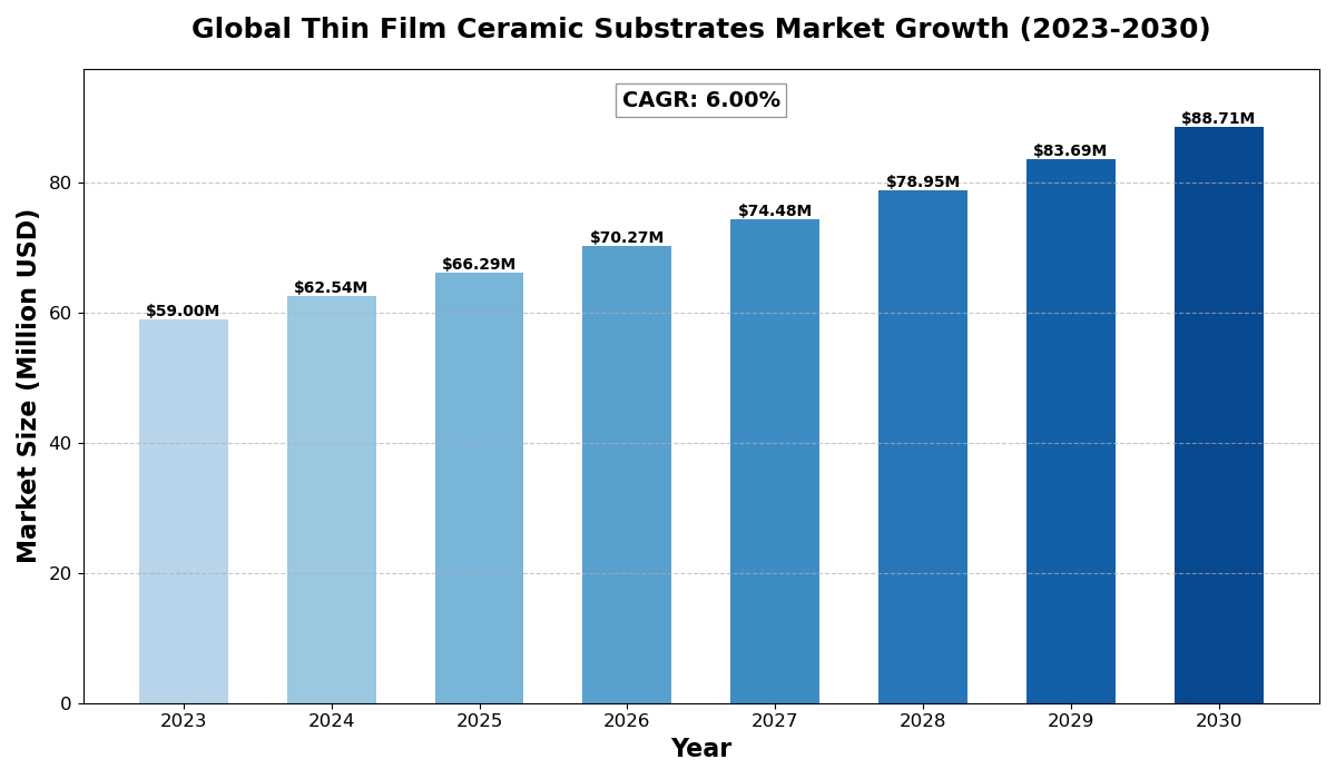
The global Thin Film Ceramic Substrates in Electronic Packaging Market size was estimated at USD 59 million in 2023 and is projected to reach USD 88.71 million by 2030, exhibiting a CAGR of 6.00% during the forecast period.
North America Thin Film Ceramic Substrates in Electronic Packaging market size was USD 15.37 million in 2023, at a CAGR of 5.14% during the forecast period of 2025 through 2030.
Thin Film Ceramic Substrates in Electronic Packaging Key Market Trends :
- Growing Demand for Miniaturization
The rising need for compact and high-performance electronic devices is driving the demand for thin film ceramic substrates, especially in applications like RF communication and LED packaging. - Advancements in Ceramic Material Technologies
Continuous innovations in Alumina (Al2O3) and Aluminum Nitride (AlN) thin film technologies are improving thermal conductivity, reliability, and performance in electronic packaging. - Increasing Adoption in 5G and IoT Devices
The expansion of 5G infrastructure and IoT-based applications is fueling the growth of thin film ceramic substrates for high-frequency and high-power applications. - Rising Investments in Semiconductor Packaging
With the increasing demand for efficient heat dissipation solutions, the semiconductor industry is significantly investing in advanced ceramic packaging solutions. - Surging Demand in Automotive Electronics
The rise of electric vehicles (EVs) and advanced driver-assistance systems (ADAS) is driving the need for durable and high-performance ceramic substrates in automotive applications.
Thin Film Ceramic Substrates in Electronic Packaging Market Regional Analysis :

-
North America:
Strong demand driven by EVs, 5G infrastructure, and renewable energy, with the U.S. leading the market.
-
Europe:
Growth fueled by automotive electrification, renewable energy, and strong regulatory support, with Germany as a key player.
-
Asia-Pacific:
Dominates the market due to large-scale manufacturing in China and Japan, with growing demand from EVs, 5G, and semiconductors.
-
South America:
Emerging market, driven by renewable energy and EV adoption, with Brazil leading growth.
-
Middle East & Africa:
Gradual growth, mainly due to investments in renewable energy and EV infrastructure, with Saudi Arabia and UAE as key contributors.
Thin Film Ceramic Substrates in Electronic Packaging Market Segmentation :
The research report includes specific segments by region (country), manufacturers, Type, and Application. Market segmentation creates subsets of a market based on product type, end-user or application, Geographic, and other factors. By understanding the market segments, the decision-maker can leverage this targeting in the product, sales, and marketing strategies. Market segments can power your product development cycles by informing how you create product offerings for different segments.
Key Company
- Maruwa
- Toshiba Materials
- Kyocera
- Vishay
- Cicor Group
- Murata
- ECRIM
- Tecdia
- Jiangxi Lattice Grand Advanced Material Technology
- CoorsTek
Market Segmentation (by Type)
- Alumina Thin Film Ceramic Substrates
- AlN Thin Film Ceramic Substrates
Market Segmentation (by Application)
- LED
- Laser Diodes
- RF and Optical Communication
- Others
Drivers:
- Rising Demand for High-Performance Electronics
The increasing need for miniaturized, high-power, and energy-efficient electronics is propelling the adoption of thin film ceramic substrates. - Growing Semiconductor Industry
The continuous expansion of the semiconductor industry, particularly in regions like Asia-Pacific, is boosting the demand for advanced electronic packaging solutions. - Enhanced Thermal and Electrical Properties
Thin film ceramic substrates offer superior thermal conductivity and electrical insulation, making them ideal for applications requiring high reliability.
Restraints:
- High Manufacturing Costs
The production process of thin film ceramic substrates involves high costs, making them expensive compared to traditional substrate materials. - Limited Adoption in Cost-Sensitive Markets
Developing regions with cost-sensitive electronic markets may prefer low-cost alternatives, hindering widespread adoption. - Complex Fabrication Process
The manufacturing of these substrates involves intricate deposition and etching processes, making mass production challenging.
Opportunities:
- Expansion in Renewable Energy Applications
Thin film ceramic substrates are increasingly being used in power electronics for renewable energy applications, opening new market opportunities. - Rising Demand in Aerospace & Defense
The need for high-reliability electronic packaging in aerospace and defense applications is creating growth opportunities. - Development of Advanced Materials
Innovations in ceramic materials and deposition technologies are expected to enhance the performance and cost-effectiveness of thin film substrates.
Challenges:
- Intense Market Competition
The presence of established players and emerging competitors makes it challenging for new entrants to gain market share. - Supply Chain Disruptions
Global supply chain issues, including raw material shortages and logistics constraints, may affect market growth. - Stringent Industry Regulations
Compliance with regulatory standards and environmental guidelines can pose challenges for manufacturers.
Key Benefits of This Market Research:
- Industry drivers, restraints, and opportunities covered in the study
- Neutral perspective on the market performance
- Recent industry trends and developments
- Competitive landscape & strategies of key players
- Potential & niche segments and regions exhibiting promising growth covered
- Historical, current, and projected market size, in terms of value
- In-depth analysis of the Thin Film Ceramic Substrates in Electronic Packaging Market
- Overview of the regional outlook of the Thin Film Ceramic Substrates in Electronic Packaging Market:
Key Reasons to Buy this Report:
- Access to date statistics compiled by our researchers. These provide you with historical and forecast data, which is analyzed to tell you why your market is set to change
- This enables you to anticipate market changes to remain ahead of your competitors
- You will be able to copy data from the Excel spreadsheet straight into your marketing plans, business presentations, or other strategic documents
- The concise analysis, clear graph, and table format will enable you to pinpoint the information you require quickly
- Provision of market value (USD Billion) data for each segment and sub-segment
- Indicates the region and segment that is expected to witness the fastest growth as well as to dominate the market
- Provides insight into the market through Value Chain
- Market dynamics scenario, along with growth opportunities of the market in the years to come
- 6-month post-sales analyst support
Customization of the Report
In case of any queries or customization requirements, please connect with our sales team, who will ensure that your requirements are met.
FAQs
Q: What are the key driving factors and opportunities in the Thin Film Ceramic Substrates in Electronic Packaging market?
A: The market is driven by the growing demand for miniaturized electronics, advancements in ceramic materials, and increasing adoption in 5G and IoT applications. Opportunities lie in renewable energy, aerospace, and defense applications.
Q: Which region is projected to have the largest market share?
A: Asia-Pacific is expected to dominate the market, driven by the booming semiconductor industry, high demand for consumer electronics, and rapid advancements in automotive technology.
Q: Who are the top players in the global Thin Film Ceramic Substrates in Electronic Packaging market?
A: Key players include Maruwa, Toshiba Materials, Kyocera, Vishay, Cicor Group, Murata, ECRIM, Tecdia, Jiangxi Lattice Grand Advanced Material Technology, and CoorsTek.
Q: What are the latest technological advancements in the industry?
A: Recent advancements include improved deposition techniques for higher efficiency, the development of high thermal conductivity substrates, and the integration of ceramic substrates in emerging applications like quantum computing.
Q: What is the current size of the global Thin Film Ceramic Substrates in Electronic Packaging market?
A: The market was valued at USD 59 million in 2023 and is projected to reach USD 88.71 million by 2030, growing at a CAGR of 6.00% during the forecast period.

Get Sample Report PDF for Exclusive Insights
Report Sample Includes
- Table of Contents
- List of Tables & Figures
- Charts, Research Methodology, and more...


