
MARKET INSIGHTS
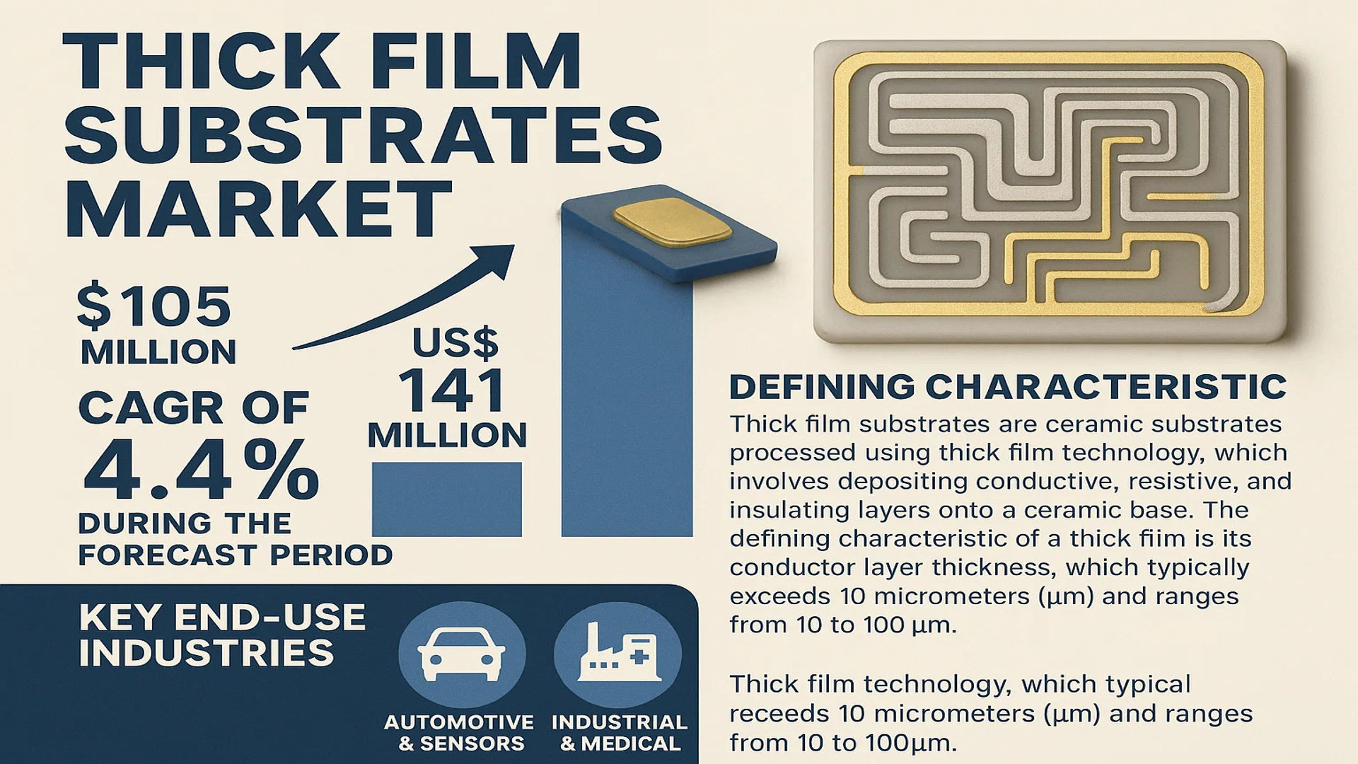
The global Thick Film Substrates Market was valued at 105 million in 2024 and is projected to reach US$ 141 million by 2032, at a CAGR of 4.4% during the forecast period.
Thick film substrates are ceramic substrates processed using thick film technology, which involves depositing conductive, resistive, and insulating layers onto a ceramic base through printing and high-temperature sintering. The defining characteristic of a thick film is its conductor layer thickness, which typically exceeds 10 micrometers (µm) and ranges from 10 to 100µm. This makes it thicker than thin-film sputtering technologies but thinner than direct bonded copper (DBC) or standard FR4 boards. These substrates are integral components in a wide array of electronic packages, particularly where high graphics accuracy is not a primary requirement, due to their mature technology, simple manufacturing process, and cost-effectiveness.
The market’s steady growth is underpinned by the robust demand from key end-use industries, most notably automotive & sensors and industrial & medical applications. The Asia-Pacific region dominates the global landscape, accounting for approximately 37% of the market share, driven by strong manufacturing and electronics sectors in China, Japan, and South Korea. The market is moderately consolidated, with the top six players—including Noritake, NCI, and Kyocera—holding a collective share of about 42% in 2024. Product-wise, alumina (Al2O3) thick film substrates are the most prevalent, commanding a 77% share of the market.
MARKET DYNAMICS
MARKET DRIVERS
Expansion of Automotive Electronics and Sensor Applications to Drive Market Growth
The global automotive industry is undergoing a significant transformation towards electrification, automation, and connectivity, which is driving substantial demand for thick film substrates. These substrates are essential components in various automotive applications, including engine control units, airbag systems, anti-lock braking systems, and advanced driver-assistance systems (ADAS). The increasing integration of electronic systems in vehicles, coupled with the rising adoption of electric vehicles (EVs), is creating robust demand for reliable and high-performance thick film ceramic substrates. The automotive electronics market is projected to grow at a compound annual growth rate of approximately 7.5%, directly influencing the thick film substrates market. Furthermore, the growing emphasis on vehicle safety regulations worldwide is mandating the incorporation of sophisticated sensor systems, which extensively utilize thick film technology for their durability and thermal management capabilities.
Growing Demand for Industrial Automation and Medical Devices to Boost Market Expansion
Industrial automation and medical device manufacturing represent significant growth areas for thick film substrates. The ongoing Industry 4.0 revolution is driving increased adoption of automation technologies across manufacturing sectors, requiring robust electronic components that can withstand harsh industrial environments. Thick film substrates offer excellent thermal stability, chemical resistance, and reliability under extreme conditions, making them ideal for industrial control systems, power modules, and sensor applications. Simultaneously, the medical device industry is experiencing substantial growth, particularly in diagnostic equipment, patient monitoring systems, and implantable devices. The global medical device market is expected to reach approximately $600 billion by 2025, creating substantial opportunities for thick film substrate manufacturers. These substrates are particularly valued in medical applications for their biocompatibility, precision, and ability to maintain performance in sterilized environments.
Advancements in LED Packaging and Power Electronics to Fuel Market Development
The rapid evolution of LED technology and power electronics is creating new opportunities for thick film substrates. The global LED market continues to expand, driven by energy efficiency initiatives and the transition to solid-state lighting. Thick film substrates provide excellent thermal management solutions for high-power LED packages, enabling better heat dissipation and longer operational life. Additionally, the power electronics sector is experiencing significant growth due to renewable energy integration, electric vehicle adoption, and industrial power conversion requirements. Thick film ceramic substrates, particularly those using aluminum nitride (AlN), offer superior thermal conductivity compared to traditional materials, making them essential for high-power applications. The power electronics market is projected to grow at approximately 6.8% annually, directly supporting the demand for advanced thick film substrates that can handle higher power densities and operating temperatures.
MARKET RESTRAINTS
High Manufacturing Costs and Intense Competition from Alternative Technologies to Limit Market Growth
Despite the growing demand, the thick film substrates market faces significant challenges related to manufacturing costs and competitive pressure from alternative technologies. The production process for thick film ceramic substrates involves multiple sophisticated steps including screen printing, drying, and high-temperature firing, which require specialized equipment and controlled environments. The capital investment for establishing manufacturing facilities can exceed $20 million for medium-scale operations, creating substantial barriers to entry and limiting market expansion. Additionally, raw material costs, particularly for specialized ceramics like aluminum nitride and beryllium oxide, remain relatively high due to complex processing requirements and limited supplier bases. These cost factors make thick film substrates less competitive in price-sensitive applications, where alternatives such as direct bonded copper (DBC) substrates or organic substrates might be preferred despite potential performance compromises.
Technical Limitations in Miniaturization and High-Frequency Applications to Restrain Market Potential
The thick film technology faces inherent limitations in meeting the demands of increasingly miniaturized electronic components and high-frequency applications. While thick film substrates excel in power handling and thermal management, their line resolution and registration accuracy are generally inferior to thin film technologies. The typical feature size achievable with thick film processing is limited to approximately 50-100 micrometers, which may not satisfy the requirements for advanced microelectronics packaging where feature sizes are shrinking below 20 micrometers. Furthermore, thick film materials exhibit higher dielectric losses at microwave frequencies compared to specialized low-loss substrates, restricting their use in high-frequency communication systems and radar applications. These technical constraints are particularly relevant in emerging 5G infrastructure and aerospace applications, where performance requirements often exceed the capabilities of conventional thick film substrates.
Environmental Regulations and Material Availability Concerns to Impede Market Expansion
Environmental regulations and material availability present additional challenges for the thick film substrates market. Certain materials used in thick film formulations, particularly those containing lead, cadmium, or other heavy metals, face increasing regulatory restrictions under environmental directives such as RoHS and REACH. The industry is transitioning to lead-free and environmentally friendly formulations, but these alternatives often involve performance trade-offs and higher material costs. Additionally, beryllium oxide, valued for its exceptional thermal conductivity, faces supply chain challenges due to health and safety concerns associated with beryllium dust inhalation during processing. The limited number of qualified beryllium oxide suppliers and increasing regulatory scrutiny are creating supply chain vulnerabilities and cost pressures for manufacturers relying on this material for high-performance applications.
MARKET CHALLENGES
Supply Chain Vulnerabilities and Raw Material Price Volatility to Challenge Market Stability
The thick film substrates market is experiencing significant supply chain challenges that impact production stability and cost structures. The industry relies on specialized raw materials including ceramic powders, precious metal pastes, and glass frits, which are subject to price volatility and supply disruptions. Recent global events have highlighted vulnerabilities in the supply chain, with lead times for certain critical materials extending beyond six months in some cases. Precious metal prices, particularly for silver and palladium used in conductor pastes, have shown volatility of up to 30% annually, creating pricing uncertainty for manufacturers and customers alike. Additionally, the geographic concentration of raw material production, with key suppliers located in specific regions, creates dependency risks that can disrupt manufacturing operations and affect market stability.
Other Challenges
Technological Transition Pressures
The rapid pace of technological change in end-use applications creates constant pressure for thick film substrate manufacturers to innovate and adapt. As electronic devices become more sophisticated, requirements for higher thermal performance, better reliability, and increased integration density are constantly evolving. Manufacturers must invest significantly in research and development to keep pace with these demands, while simultaneously maintaining cost competitiveness. The transition to new materials systems, such as the development of low-temperature co-fired ceramic (LTCC) alternatives and advanced thermal interface materials, requires substantial capital investment and technical expertise that may be challenging for smaller market participants.
Quality Consistency and Production Yield Issues
Maintaining consistent quality and high production yields remains a persistent challenge in thick film substrate manufacturing. The multi-step production process involves numerous variables that can affect final product quality, including paste composition, printing parameters, drying conditions, and firing profiles. Even minor variations in these parameters can lead to defects such as delamination, cracking, or electrical performance issues. Achieving production yields above 95% consistently remains challenging for complex multilayer designs, particularly when manufacturing larger panel sizes or incorporating fine features. These quality control challenges become more pronounced as customer requirements for reliability and performance specifications become increasingly stringent.
MARKET OPPORTUNITIES
Emerging Applications in Renewable Energy and Electric Vehicle Infrastructure to Create New Growth Avenues
The global transition toward renewable energy and electric mobility is creating substantial opportunities for thick film substrate manufacturers. Solar inverters, wind power converters, and energy storage systems require robust power electronic components that can operate reliably under demanding environmental conditions. Thick film substrates, with their excellent thermal management properties and high reliability, are ideally suited for these applications. The solar inverter market alone is projected to grow at approximately 8% annually, driven by increasing solar installations worldwide. Similarly, the electric vehicle charging infrastructure market is expanding rapidly, with estimates suggesting installation growth rates exceeding 30% per year. These applications demand power electronics capable of handling high voltages and currents while maintaining efficiency, creating significant opportunities for advanced thick film substrates in power conversion and management systems.
Advancements in 5G Infrastructure and IoT Devices to Open New Market Frontiers
The deployment of 5G networks and proliferation of Internet of Things (IoT) devices are creating new application areas for thick film substrates. While traditional thick film technology has limitations in high-frequency applications, recent advancements in material science and processing techniques are enabling their use in certain RF and microwave components. Base station power amplifiers, antenna systems, and RF front-end modules can benefit from the thermal management capabilities of thick film substrates. Additionally, the growing IoT market, expected to connect over 30 billion devices by 2025, requires cost-effective and reliable electronic packaging solutions for sensors, communication modules, and edge computing devices. Thick film technology offers a compelling combination of performance and cost efficiency for these applications, particularly in industrial and automotive IoT segments where environmental robustness is critical.
Geographic Expansion and Strategic Partnerships to Enhance Market Position
Significant opportunities exist for thick film substrate manufacturers through geographic expansion and strategic partnerships. The Asia-Pacific region, particularly China, Japan, and South Korea, represents the largest and fastest-growing market for electronic components. Establishing manufacturing facilities or partnerships in these regions can provide access to growing local demand and potentially lower production costs. Several major players have announced expansion plans in Southeast Asia, with investment commitments exceeding $100 million collectively over the next three years. Additionally, strategic partnerships with end-users and technology developers can create opportunities for customized solutions and early involvement in new product development. Collaborations with automotive tier-one suppliers, medical device manufacturers, and industrial equipment producers are particularly valuable for developing application-specific substrates that address unique performance requirements and create differentiated market positions.
THICK FILM SUBSTRATES MARKET TRENDS
Rising Demand for Automotive Electronics and Sensors Drives Market Expansion
The proliferation of advanced driver-assistance systems (ADAS), electric vehicles (EVs), and in-vehicle infotainment systems is significantly boosting the demand for thick film substrates globally. These substrates provide excellent thermal management, high electrical insulation, and reliable performance in harsh automotive environments, making them indispensable for sensor applications, power modules, and control units. The global automotive sensor market, a key consumer, is projected to exceed $40 billion by 2030, directly correlating with increased consumption of alumina-based thick film circuits. Furthermore, the transition towards autonomous driving, which relies on a complex network of LiDAR, radar, and ultrasonic sensors, necessitates robust and durable electronic packaging that thick film technology is uniquely positioned to provide. This trend is most pronounced in the Asia-Pacific region, which holds a 37% market share and is home to the world’s largest automotive manufacturing hubs.
Other Trends
Miniaturization and High-Density Integration in Power Electronics
The relentless push for miniaturization across consumer electronics, telecommunications, and industrial equipment is compelling manufacturers to adopt thick film substrates for their ability to host integrated passive components, such as resistors and capacitors, directly onto the ceramic surface. This integration reduces the overall footprint and enhances circuit reliability by minimizing solder joints and interconnects. The market for power devices, which accounted for a significant segment of application in 2024, is increasingly utilizing Aluminum Nitride (AlN) thick film substrates due to their superior thermal conductivity, which is approximately 10 times higher than that of standard alumina. This is critical for managing heat dissipation in high-power applications like IGBT modules and RF power amplifiers, ensuring longer product lifecycles and improved performance.
Strategic Focus on Advanced Material Development and Regional Supply Chain Consolidation
Leading manufacturers are heavily investing in R&D to develop next-generation materials that offer enhanced thermal and mechanical properties. While alumina dominates the market with a 77% share by product type, there is growing interest in AlN and BeO substrates for niche, high-performance applications in aerospace, defense, and advanced medical imaging equipment. However, the market remains constrained by the high cost and processing complexity of these advanced ceramics. Concurrently, the industry is witnessing a strategic consolidation of manufacturing capacities within the Asia-Pacific region to capitalize on lower production costs and proximity to key end-user industries. This regional dominance is reinforced by the fact that the top six players collectively hold 42% of the global market, with several key players based in Japan and the US actively forming partnerships and expanding production facilities in China and Southeast Asia to secure their supply chains and cater to local demand.
COMPETITIVE LANDSCAPE
Key Industry Players
Technological Innovation and Strategic Expansion Drive Market Leadership
The global thick film substrates market exhibits a semi-consolidated competitive structure, characterized by the presence of several established multinational corporations alongside numerous specialized regional manufacturers. Noritake Co., Limited (Japan) is a dominant force, leveraging its extensive experience in ceramic technology and a robust global distribution network. The company’s leadership is further solidified by its significant investments in research and development, particularly in enhancing the thermal and electrical performance of its alumina substrates, which command the largest product segment share.
Kyocera Corporation (Japan) and NCI (USA) also hold substantial market shares, collectively accounting for a significant portion of global revenues. Kyocera’s strength lies in its vertically integrated manufacturing processes and diverse application reach, from automotive sensors to advanced power modules. NCI, meanwhile, has carved a strong niche in the North American market through its high-reliability substrates for demanding industrial and military applications. The growth trajectories of these companies are intrinsically linked to their ability to innovate in material science and respond to the increasing miniaturization and performance requirements of modern electronics.
Furthermore, these industry leaders are actively pursuing growth through strategic initiatives. This includes geographical expansion into high-growth regions like Asia-Pacific, which represents the largest market, and through mergers and acquisitions to bolster technological portfolios and manufacturing capabilities. New product launches focusing on advanced materials like Aluminum Nitride (AlN) for better thermal management are a key competitive differentiator.
Meanwhile, other significant players such as Maruwa Co., Ltd. (Japan) and Cicor Group (Switzerland) are strengthening their positions. Maruwa is renowned for its high-quality substrates used in RF and microwave applications, while Cicor has been expanding its footprint through strategic acquisitions, such as its purchase of MST (Micro Systems Technologies), to enhance its offering in the medical and aerospace sectors. These companies, along with others, are ensuring a dynamic and evolving competitive landscape through sustained R&D investment and strategic market positioning.
List of Key Thick Film Substrates Companies Profiled
- Noritake Co., Limited (Japan)
- NCI (USA)
- Kyocera Corporation (Japan)
- Miyoshi Electronics Corporation (Japan)
- CMS Circuits, Inc (USA)
- Cicor Group (Switzerland)
- Maruwa Co., Ltd. (Japan)
- Nikko Company (Japan)
- APITech (CMAC) (USA)
- Mitsuboshi Belting Ltd. (Japan)
Segment Analysis:
By Type
Alumina Thick Film Substrates Segment Dominates the Market Due to Cost-Effectiveness and Mature Manufacturing Processes
The market is segmented based on type into:
- Alumina (Al2O3) Thick Film Substrates
- Aluminum Nitride (AlN) Thick Film Substrates
- Beryllium Oxide (BeO) Thick Film Substrates
- Others
By Application
Automotive & Sensors Segment Leads Due to Growing Demand for Electronic Control Units and Sensor Integration
The market is segmented based on application into:
- Automotive & Sensors
- Industrial & Medical
- Power Devices
- LEDs
- MEMS Packages
- Military & Defence
- Others
By End-User Industry
Electronics Manufacturing Segment Holds Significant Share Due to Widespread Use in Circuit Board Production
The market is segmented based on end-user industry into:
- Electronics Manufacturing
- Automotive
- Healthcare & Medical Devices
- Aerospace & Defense
- Telecommunications
- Others
By Manufacturing Process
Screen Printing Segment Prevails as the Primary Manufacturing Method Due to its Efficiency and Scalability
The market is segmented based on manufacturing process into:
- Screen Printing
- Photolithography
- Laser Processing
- Others
Regional Analysis: Thick Film Substrates Market
Asia-Pacific
Asia-Pacific is the dominant region in the global thick film substrates market, holding approximately 37% of the market share. This leadership is driven by robust demand from key manufacturing hubs including China, Japan, and South Korea. The region benefits from extensive electronics production capabilities, strong government support for industrial growth, and significant investments in automotive and consumer electronics sectors. China’s “Made in China 2025” initiative, for instance, continues to bolster advanced manufacturing, including the production of electronic components that utilize thick film substrates. Japan remains a technological leader with companies like Noritake and Kyocera driving innovation, while South Korea’s strong semiconductor and display industries further fuel demand. The widespread adoption of these substrates in automotive sensors, industrial controls, and LED applications underpins the region’s growth. However, cost sensitivity in certain segments and increasing environmental regulations pose challenges, though the market continues to expand due to urbanization and technological advancement.
North America
North America represents a significant and technologically advanced market for thick film substrates, characterized by high demand for precision and reliability in critical applications. The region’s strong aerospace, defense, and medical device industries drive the need for high-performance substrates that meet stringent quality standards. The presence of key players such as CMS Circuits, Inc. and TTM Technologies supports local supply chains and innovation. Recent U.S. legislation, including the CHIPS and Science Act, which allocates funding for semiconductor research and production, indirectly benefits the thick film substrates market by promoting domestic electronics manufacturing. Additionally, the growing adoption of electric vehicles and advanced driver-assistance systems (ADAS) in the automotive sector is creating new opportunities. While the market is mature, ongoing investments in next-generation technologies and a focus on miniaturization and efficiency ensure steady growth.
Europe
Europe holds a substantial share of the thick film substrates market, supported by a strong industrial base and emphasis on high-quality manufacturing. The region’s well-established automotive industry, particularly in Germany, is a major consumer, using these substrates in various sensors and control units. Strict environmental regulations under EU directives encourage the development and adoption of efficient and compliant electronic components. Companies like Cicor Group and MST (Micro Systems Technologies) are key contributors, focusing on innovation and customized solutions for medical, automotive, and industrial applications. Europe’s commitment to renewable energy and smart grid technologies also drives demand in power device applications. However, high production costs and competition from Asian manufacturers present challenges, though the region’s focus on quality and reliability helps maintain its competitive edge.
South America
The thick film substrates market in South America is emerging, with growth primarily driven by industrial expansion and increasing electronics production in countries like Brazil and Argentina. The region’s automotive and consumer electronics sectors are gradually adopting these substrates, though market penetration remains lower compared to more developed regions. Economic volatility and limited local manufacturing capabilities for advanced electronic components often lead to reliance on imports, which can affect cost and supply chain stability. However, government initiatives to boost industrial output and technological adoption are creating opportunities. The market is characterized by a focus on cost-effective solutions, with potential for growth as regional infrastructure and investment in electronics manufacturing improve.
Middle East & Africa
The Middle East & Africa region is in the early stages of adopting thick film substrates, with demand primarily emerging from telecommunications, energy, and limited industrial applications. Countries like Israel, Turkey, and the UAE are showing increased interest in advanced electronics as part of broader economic diversification efforts. The region’s growing investment in smart city projects and infrastructure development presents potential opportunities for thick film substrates in sensors and control systems. However, the market faces significant challenges, including limited local manufacturing, reliance on imports, and underdeveloped regulatory frameworks for electronic components. While the current market size is small, long-term growth potential exists as technological adoption increases and industrial capabilities expand.
Report Scope
This market research report provides a comprehensive analysis of the global and regional Thick Film Substrates markets, covering the forecast period 2025–2032. It offers detailed insights into market dynamics, technological advancements, competitive landscape, and key trends shaping the industry.
Key focus areas of the report include:
- Market Size & Forecast: Historical data and future projections for revenue, unit shipments, and market value across major regions and segments.
- Segmentation Analysis: Detailed breakdown by product type, technology, application, and end-user industry to identify high-growth segments and investment opportunities.
- Regional Outlook: Insights into market performance across North America, Europe, Asia-Pacific, Latin America, and the Middle East & Africa, including country-level analysis where relevant.
- Competitive Landscape: Profiles of leading market participants, including their product offerings, R&D focus, manufacturing capacity, pricing strategies, and recent developments such as mergers, acquisitions, and partnerships.
- Technology Trends & Innovation: Assessment of emerging technologies, integration of AI/IoT, semiconductor design trends, fabrication techniques, and evolving industry standards.
- Market Drivers & Restraints: Evaluation of factors driving market growth along with challenges, supply chain constraints, regulatory issues, and market-entry barriers.
- Stakeholder Analysis: Insights for component suppliers, OEMs, system integrators, investors, and policymakers regarding the evolving ecosystem and strategic opportunities.
Primary and secondary research methods are employed, including interviews with industry experts, data from verified sources, and real-time market intelligence to ensure the accuracy and reliability of the insights presented.
FREQUENTLY ASKED QUESTIONS:
What is the current market size of Global Thick Film Substrates Market?
-> Thick Film Substrates Market was valued at 105 million in 2024 and is projected to reach US$ 141 million by 2032, at a CAGR of 4.4% during the forecast period.
Which key companies operate in Global Thick Film Substrates Market?
-> Key players include Noritake, NCI, Miyoshi Electronics Corporation, Kyocera, CMS Circuits, Inc, Cicor Group, Maruwa, Nikko, APITech (CMAC), and Mitsuboshi Belting, among others.
What are the key growth drivers?
-> Key growth drivers include increasing demand from automotive sensors, industrial applications, and the expansion of LED and power device markets.
Which region dominates the market?
-> Asia-Pacific is the largest market with approximately 37% share, driven by strong demand from China, Japan, and South Korea.
What are the emerging trends?
-> Emerging trends include advancements in AlN and BeO substrate technologies, miniaturization of electronic components, and increased adoption in MEMS packages and military applications.

Get Sample Report PDF for Exclusive Insights
Report Sample Includes
- Table of Contents
- List of Tables & Figures
- Charts, Research Methodology, and more...



