Semiconductor Wafer Electrostatic Chucks for 300mm Wafer Market Overview
Electrostatic chuck, has been widely used in semiconductor process in plasma and vacuum environment, such as etching, chemical vapor deposition, ion implantation, etc. The advantages of this technology lie in its improvement of yield, no edge elimination effect of wafer, good wafer holding uniformity, controllable temperature, etc. A typical electrostatic chuck clamping system is a sandwich structure consisting of three parts: dielectric adsorption layer, electrode layer, and base layer. The three parts are stacked in the electrostatic chuck in a layered structure. From the surface to the base, they are dielectric adsorption layer, electrode layer, and base layer. Compared with traditional mechanical chuck and vacuum chuck, electrostatic chuck has many advantages. Therefore, electrostatic chuck has replaced the traditional mechanical chuck and vacuum chuck, and is widely used in integrated circuit manufacturing process. This report studies the semiconductor wafer electrostatic chuck for 300mm wafer.
This report provides a deep insight into the global Semiconductor Wafer Electrostatic Chucks for 300mm Wafer market covering all its essential aspects. This ranges from a macro overview of the market to micro details of the market size, competitive landscape, development trend, niche market, key market drivers and challenges, SWOT analysis, value chain analysis, etc.
The analysis helps the reader to shape the competition within the industries and strategies for the competitive environment to enhance the potential profit. Furthermore, it provides a simple framework for evaluating and accessing the position of the business organization. The report structure also focuses on the competitive landscape of the Global Semiconductor Wafer Electrostatic Chucks for 300mm Wafer Market, this report introduces in detail the market share, market performance, product situation, operation situation, etc. of the main players, which helps the readers in the industry to identify the main competitors and deeply understand the competition pattern of the market.
In a word, this report is a must-read for industry players, investors, researchers, consultants, business strategists, and all those who have any kind of stake or are planning to foray into the Semiconductor Wafer Electrostatic Chucks for 300mm Wafer market in any manner.
Semiconductor Wafer Electrostatic Chucks for 300mm Wafer Market Analysis:
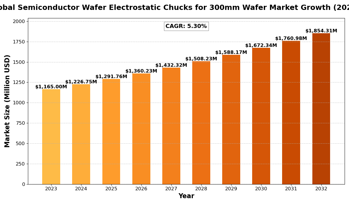
The global Semiconductor Wafer Electrostatic Chucks for 300mm Wafer Market size was estimated at USD 1165 million in 2023 and is projected to reach USD 1854.31 million by 2032, exhibiting a CAGR of 5.30% during the forecast period.
North America Semiconductor Wafer Electrostatic Chucks for 300mm Wafer market size was estimated at USD 331.77 million in 2023, at a CAGR of 4.54% during the forecast period of 2025 through 2032.
Semiconductor Wafer Electrostatic Chucks for 300mm Wafer Key Market Trends :
-
Growing Adoption of 300mm Wafers
The semiconductor industry is shifting towards 300mm wafers due to cost efficiency and increased chip production per wafer, driving demand for electrostatic chucks. -
Advancements in Electrostatic Chuck Technology
Enhanced materials and innovative cooling mechanisms are improving wafer handling precision, temperature control, and reducing contamination risks. -
Rising Demand for Semiconductor Equipment
The expanding semiconductor manufacturing sector, driven by AI, IoT, and 5G technologies, is boosting the need for electrostatic chucks. -
Expansion of Foundries in Asia-Pacific
Countries like China, Taiwan, and South Korea are heavily investing in semiconductor fabrication plants, fueling market growth. -
Sustainability and Energy Efficiency Focus
Manufacturers are emphasizing energy-efficient designs and sustainable production processes to align with environmental regulations.
Semiconductor Wafer Electrostatic Chucks for 300mm Wafer Market Regional Analysis :

-
North America:
Strong demand driven by EVs, 5G infrastructure, and renewable energy, with the U.S. leading the market.
-
Europe:
Growth fueled by automotive electrification, renewable energy, and strong regulatory support, with Germany as a key player.
-
Asia-Pacific:
Dominates the market due to large-scale manufacturing in China and Japan, with growing demand from EVs, 5G, and semiconductors.
-
South America:
Emerging market, driven by renewable energy and EV adoption, with Brazil leading growth.
-
Middle East & Africa:
Gradual growth, mainly due to investments in renewable energy and EV infrastructure, with Saudi Arabia and UAE as key contributors.
Semiconductor Wafer Electrostatic Chucks for 300mm Wafer Market Segmentation :
The research report includes specific segments by region (country), manufacturers, Type, and Application. Market segmentation creates subsets of a market based on product type, end-user or application, Geographic, and other factors. By understanding the market segments, the decision-maker can leverage this targeting in the product, sales, and marketing strategies. Market segments can power your product development cycles by informing how you create product offerings for different segments.
Key Company
- Applied Materials
- Lam Research
- SHINKO
- TOTO
- Creative Technology Corporation
- Kyocera
- NGK Insulators
- Ltd.
- NTK CERATEC
- Tsukuba Seiko
- II-VI M Cubed
Market Segmentation (by Type)
- Coulomb Type Electrostatic Chucks
- Johnsen-Rahbek(JR) Type Electrostatic Chucks
Market Segmentation (by Application)
- Wafer Supplier
- Original Manufacturer of Semiconductor Equipment
Market Drivers
-
Growing Semiconductor Industry
The increasing adoption of AI, IoT, and 5G is fueling semiconductor production, driving demand for electrostatic chucks. -
Shift to 300mm Wafers
Manufacturers prefer larger wafers for higher production efficiency and reduced costs, boosting the electrostatic chuck market. -
Technological Advancements
Improved materials, temperature control, and contamination prevention technologies enhance electrostatic chuck performance.
Market Restraints
-
High Initial Investment
The cost of advanced electrostatic chuck systems and semiconductor manufacturing equipment is a major barrier for new entrants. -
Complex Manufacturing Process
Electrostatic chucks require precision engineering and high-quality materials, making production challenging and costly. -
Supply Chain Disruptions
Geopolitical tensions, raw material shortages, and global trade issues impact the steady supply of semiconductor components.
Market Opportunities
-
Growing Demand in AI & IoT Applications
Increased adoption of AI-driven devices and IoT solutions is boosting semiconductor manufacturing, creating new opportunities. -
Expansion in Emerging Markets
Developing countries are investing in semiconductor fabrication plants, increasing demand for electrostatic chucks. -
Advancements in Material Science
Research in dielectric materials and better cooling techniques is enhancing electrostatic chuck efficiency and durability.
Market Challenges
-
Stringent Industry Regulations
Semiconductor manufacturing involves strict environmental and safety regulations, adding compliance challenges. -
Intense Market Competition
Major players are continuously innovating, making it challenging for smaller companies to establish a foothold. -
Rapid Technological Changes
Frequent advancements in semiconductor processes require continuous upgrades in electrostatic chuck technology.
Key Benefits of This Market Research:
- Industry drivers, restraints, and opportunities covered in the study
- Neutral perspective on the market performance
- Recent industry trends and developments
- Competitive landscape & strategies of key players
- Potential & niche segments and regions exhibiting promising growth covered
- Historical, current, and projected market size, in terms of value
- In-depth analysis of the Semiconductor Wafer Electrostatic Chucks for 300mm Wafer Market
- Overview of the regional outlook of the Semiconductor Wafer Electrostatic Chucks for 300mm Wafer Market:
Key Reasons to Buy this Report:
- Access to date statistics compiled by our researchers. These provide you with historical and forecast data, which is analyzed to tell you why your market is set to change
- This enables you to anticipate market changes to remain ahead of your competitors
- You will be able to copy data from the Excel spreadsheet straight into your marketing plans, business presentations, or other strategic documents
- The concise analysis, clear graph, and table format will enable you to pinpoint the information you require quickly
- Provision of market value data for each segment and sub-segment
- Indicates the region and segment that is expected to witness the fastest growth as well as to dominate the market
- Provides insight into the market through Value Chain
- Market dynamics scenario, along with growth opportunities of the market in the years to come
- 6-month post-sales analyst support
Customization of the Report
In case of any queries or customization requirements, please connect with our sales team, who will ensure that your requirements are met.
FAQs
Q: What are the key driving factors and opportunities in the Semiconductor Wafer Electrostatic Chucks for 300mm Wafer market?
A: The market is driven by the shift to 300mm wafers, advancements in electrostatic chuck technology, and growing demand in AI, IoT, and 5G applications. Emerging markets and innovations in materials also present opportunities.
Q: Which region is projected to have the largest market share?
A: Asia-Pacific is expected to dominate the market due to strong investments in semiconductor manufacturing in China, Taiwan, and South Korea.
Q: Who are the top players in the global Semiconductor Wafer Electrostatic Chucks for 300mm Wafer market?
A: Leading companies include Applied Materials, Lam Research, SHINKO, TOTO, Kyocera, and NGK Insulators.
Q: What are the latest technological advancements in the industry?
A: Innovations include improved dielectric materials, better cooling mechanisms, and enhanced wafer handling precision for higher efficiency.
Q: What is the current size of the global Semiconductor Wafer Electrostatic Chucks for 300mm Wafer market?
A: The market was valued at USD 1165 million in 2023 and is projected to reach USD 1854.31 million by 2032, growing at a CAGR of 5.30%.

Get Sample Report PDF for Exclusive Insights
Report Sample Includes
- Table of Contents
- List of Tables & Figures
- Charts, Research Methodology, and more...

