Semiconductor Plasma Process Monitors Market Insights
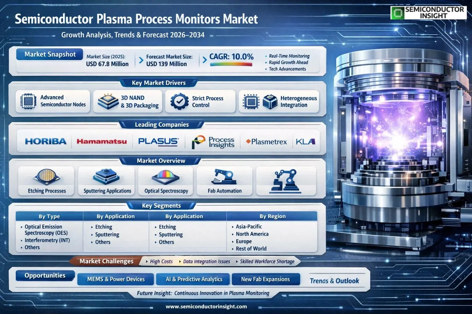
Global Semiconductor Plasma Process Monitors market size was valued at USD 67.8 million in 2025. The market is projected to grow from USD 74.6 million in 2026 to USD 139 million by 2034, exhibiting a CAGR of 10.0% during the forecast period.
Semiconductor Plasma Process Monitors are critical metrology tools used to monitor and control plasma emissions during advanced semiconductor manufacturing processes. These systems facilitate real-time analysis of plasma characteristics, enabling precise control over critical fabrication steps such as etching, sputtering, and chemical vapor deposition (CVD). The primary monitoring technologies include Optical Emission Spectroscopy (OES), Interferometry (INT), and other advanced diagnostic methods.
The market is experiencing robust growth due to several key factors, including the increasing complexity of semiconductor device nodes, the rising adoption of 3D NAND and advanced logic chips, and the stringent requirements for process control in high-volume manufacturing fabs. Furthermore, the industry’s push towards more sophisticated packaging technologies like chiplets and heterogeneous integration is creating new demand for precise plasma monitoring solutions. Initiatives by leading players are also propelling the market forward; for instance, companies are continuously integrating artificial intelligence for predictive maintenance and fault detection. Key global manufacturers operating in this space with comprehensive product portfolios include HORIBA, Hamamatsu Photonics, KLA Corporation, PLASUS GmbH, Process Insights, Plasmetrex GmbH, and Impedans Ltd.
MARKET DRIVERS
Increasing Complexity of Advanced Semiconductor Nodes
The relentless drive toward sub-5nm process technologies is a primary driver for the semiconductor plasma process monitors market. At these advanced nodes, atomic-level precision in etching and deposition is non-negotiable. Plasma process monitors provide the critical, real-time metrology needed to control parameters like ion density, radical species concentration, and etch rates, which directly impact device yield and performance. Without this advanced monitoring, achieving the uniformity and repeatability required for high-volume manufacturing would be impossible.
Growing Demand for Heterogeneous Integration and 3D Packaging
The industry’s shift toward heterogeneous integration and 3D packaging schemes, such as chiplets and through-silicon vias (TSVs), creates complex plasma processes that must be meticulously monitored. Etching high-aspect-ratio features and depositing conformal barrier layers within these intricate structures demand unparalleled process control. Semiconductor plasma process monitors are essential for ensuring process stability across these challenging new architectures, directly supporting the performance and reliability of next-generation packages.
➤ Global push for semiconductor self-sufficiency and capacity expansion is leading to the construction of hundreds of new fabrication tools, each requiring integrated plasma diagnostics to ensure optimal performance from day one.
Furthermore, stringent yield management and cost-reduction pressures compel chipmakers to implement predictive maintenance strategies. By continuously monitoring plasma health, these systems can flag tool drift or component degradation before they cause wafers to be scrapped, translating to significant operational savings and tool uptime.
MARKET CHALLENGES
Integration and Data Complexity in High-Mix Fabs
A significant challenge in the semiconductor plasma process monitors market is the seamless integration of diagnostic data into fab-wide advanced process control (APC) frameworks. Modern fabs run a high mix of products, each with unique recipes. Correlating vast, multi-parameter data streams from plasma monitors with final electrical test results to create actionable process windows requires sophisticated algorithms and significant computational resources, posing a hurdle for widespread, optimized adoption.
Other Challenges
High Cost of Ownership and ROI Justification
The advanced sensors and spectroscopic systems used in leading-edge plasma process monitors represent a substantial capital investment. For smaller fabrication facilities or older production lines, justifying this cost against perceived yield gains can be difficult, potentially slowing market penetration in these segments.
Rapid Process Development Cycles
The accelerating pace of new material and process introduction, such as the adoption of high-k dielectrics and new metal gates, requires plasma monitor technologies to be highly adaptable. Developing new optical emission spectroscopy (OES) fingerprints or refining radio frequency (RF) diagnostic algorithms for novel chemistries creates a continuous R&D burden for equipment suppliers.
MARKET RESTRAINTS
Economic Cyclicality and Capital Expenditure Volatility
The semiconductor plasma process monitors market is intrinsically tied to the capital expenditure cycles of integrated device manufacturers (IDMs) and foundries. During industry downturns or periods of overcapacity, spending on new process equipment and ancillary metrology tools is often the first to be delayed or reduced. This cyclicality can restrain steady market growth, as purchasing decisions for these advanced monitoring systems are highly sensitive to near-term financial forecasts and capacity utilization rates.
Technical Expertise and Workforce Shortages
Effectively deploying and utilizing the data from advanced semiconductor plasma process monitors requires a specialized workforce with cross-disciplinary expertise in plasma physics, data science, and semiconductor process engineering. Global shortage of such skilled technicians and engineers can act as a restraint, as fabs may be unable to fully leverage their investment, limiting the perceived value and adoption rate of the most sophisticated monitoring solutions.
MARKET OPPORTUNITIES
Expansion into Emerging Fabrication Technologies
The rise of new fabrication domains presents substantial opportunities for the semiconductor plasma process monitors market. The manufacturing of micro-electromechanical systems (MEMS), power semiconductors (like GaN and SiC), and photonic integrated circuits all rely on specialized plasma processes. Adapting monitoring technologies to meet the unique requirements of these high-growth segments—such as deeper etching for MEMS or precise surface conditioning for wide-bandgap materials—opens new application avenues beyond traditional logic and memory.
AI-Driven Predictive Analytics and Closed-Loop Control
The integration of artificial intelligence and machine learning with plasma monitoring data represents a transformative opportunity. AI algorithms can analyze complex, real-time data streams to predict endpoint detection, forecast maintenance needs, and even recommend recipe adjustments autonomously. This evolution from monitoring to intelligent, closed-loop process control can significantly enhance yield and reduce costs, creating high-value upgrade paths for existing installed tools and new system sales.
Semiconductor Plasma Process Monitors Market Trends
Rising Dominance of In-Situ Process Control
An overarching trend in the Semiconductor Plasma Process Monitors Market is the critical shift towards real-time, in-situ monitoring. As semiconductor fabrication nodes shrink to 3nm and below, the margin for error in plasma-based processes like etching and sputtering becomes virtually zero. The integration of monitors directly within the process chamber provides immediate feedback on plasma characteristics such as ion density and species concentration, allowing for instantaneous adjustments. This capability is essential for improving yield, reducing wafer scrap, and controlling costs in advanced manufacturing lines. The demand for such precision is a primary driver for market growth.
Other Trends
Adoption of Optical Emission Spectroscopy (OES)
Within the market, Optical Emission Spectroscopy (OES) has emerged as the dominant monitoring technique. OES systems analyze the light emitted by a plasma to identify chemical species and measure their concentrations. Its non-invasive nature, high sensitivity, and ability to provide multi-element analysis make it particularly suitable for the etching process, which is a major application for these monitors. Suppliers are focusing on enhancing the spectral range and data processing speed of OES-based monitors to better serve next-generation processes.
Application-Specific Monitor Development
Manufacturers in the Semiconductor Plasma Process Monitors Market are increasingly developing specialized solutions tailored to specific applications. The monitoring requirements for high-aspect-ratio silicon etching differ significantly from those for metal sputtering or complex dielectric etch processes. Leading companies are therefore offering application-specific configurations that integrate sensor technology, calibration, and software analytics optimized for distinct process steps. This trend helps semiconductor fabs achieve superior process repeatability and tighter control.
Expansion into Emerging Manufacturing Hubs
The geographic focus of market growth is following the expansion of semiconductor manufacturing capacity, particularly in the Asia-Pacific region. While established players from Japan and the U.S. lead the market, significant demand is emanating from new fabrication facilities in Southeast Asia and China. This regional growth is prompting key vendors to strengthen their sales, support, and service networks in these areas to capture the rising demand for plasma process monitoring solutions alongside major new fab investments.
COMPETITIVE LANDSCAPE
Key Industry Players
A specialized segment driven by precision, reliability, and advanced spectroscopy.
Global semiconductor plasma process monitors market is characterized by a concentrated yet dynamic competitive structure, with a handful of specialized manufacturers holding significant technological and market share. These critical tools, used to monitor plasma emissions during etching and sputtering processes, require deep expertise in Optical Emission Spectroscopy (OES), interferometry, and advanced sensor technology. HORIBA and KLA Corporation are widely recognized as market leaders, leveraging their extensive portfolios in metrology and process control to offer integrated, high-precision monitoring solutions that are essential for advanced node semiconductor manufacturing. The market’s technical complexity creates high barriers to entry, reinforcing the strong position of these established players who continuously innovate to meet the stringent demands of foundries and IDMs.
Beyond the top-tier innovators, several significant players compete by offering specialized and niche solutions that address specific monitoring challenges or provide cost-effective alternatives for particular applications. Companies such as Hamamatsu Photonics excel in providing the core photonic components and sensors, while firms like Impedans Ltd. focus on RF and plasma diagnostic solutions complementary to optical monitoring. PLASUS and Process Insights are key providers of gas analysis and compact monitoring systems, catering to specific segments of the semiconductor and adjacent industries. The competitive intensity is further heightened by the strategic focus on real-time process control and the integration of data analytics to enhance yield, pushing vendors to expand their technological capabilities and service offerings.
List of Key Semiconductor Plasma Process Monitors Companies Profiled
- HORIBA
- KLA Corporation
- Hamamatsu Photonics
- PLASUS GmbH
- Process Insights
- Plasmetrex GmbH
- Impedans Ltd.
- Advanced Energy Industries, Inc.
- MKS Instruments
- Veeco Instruments Inc.
- Nanotronics
- Cyber Technologies GmbH
- Unaxis Semiconductors (part of Oerlikon Group)
- Plasma-Therm
- Applied Materials, Inc.
Segment Analysis:
| Segment Category | Sub-Segments | Key Insights |
| By Type |
|
Optical Emission Spectroscopy (OES) is the foundational and most mature monitoring technology, prized for its real-time, non-invasive analytical capabilities. Its key strength lies in providing detailed chemical composition data from the plasma glow, which is critical for detecting endpoint and ensuring process repeatability. The technology continues to evolve with enhanced sensitivity and multi-channel detection, solidifying its dominance for advanced process control across various plasma-based fabrication steps. |
| By Application |
|
Etching represents the primary and most critical application, driving substantial demand for precise plasma monitors. The need for atomic-level precision in creating circuit patterns makes real-time plasma monitoring indispensable for controlling etch rate, selectivity, and profile. As device geometries shrink, the reliance on these monitors to prevent defects and ensure yield has intensified, making them a non-negotiable tool in advanced etching processes for leading-edge logic and memory chips. |
| By End User |
|
Foundries constitute the most significant and demanding end-user segment. Operating at the cutting edge of process technology for diverse clients, foundries prioritize maximising wafer yield and process uniformity. This creates an exceptionally high requirement for advanced plasma monitoring to ensure consistency across high-volume production runs and to rapidly diagnose process excursions. The competitive landscape among leading foundries directly fuels investment in the latest monitor technologies for a critical competitive edge. |
| By Technology Node |
|
Advanced Nodes (Below 10nm/7nm) are the primary growth engine for sophisticated plasma monitor adoption. The extreme tolerances and complex 3D structures at these nodes leave virtually no margin for process error, making in-situ plasma diagnostics mandatory rather than optional. This segment demands monitors with superior resolution, faster data acquisition, and advanced algorithms for predictive analytics, driving continuous innovation from suppliers to meet the stringent process control requirements of next-generation semiconductor manufacturing. |
| By Integration Level |
|
Integrated Process Control Systems represent the leading and most value-driven segment, moving beyond simple monitoring to closed-loop control. This integration allows for real-time adjustment of process parameters based on plasma data, which is crucial for achieving target performance metrics like etch depth and uniformity. The shift towards smart factories and full fab automation is accelerating demand for these deeply integrated solutions, as they reduce human intervention, minimize variability, and enhance overall equipment effectiveness (OEE) on the production floor. |
Regional Analysis: Semiconductor Plasma Process Monitors Market
Asia-Pacific
The density of leading-edge semiconductor fabs in Taiwan, South Korea, and Japan establishes the Asia-Pacific region as the primary market for plasma process monitors, driving both volume sales and the development of application-specific monitoring technologies for high-volume manufacturing environments.
Local manufacturers in the region are increasingly developing and supplying advanced plasma monitoring systems, reducing reliance on imports. This fosters a competitive landscape where monitors are optimized for the specific etch and deposition processes prevalent in APAC fabs.
National policies in China, Japan, and South Korea aimed at strengthening domestic semiconductor capabilities are accelerating fab expansion and upgrades. This directly fuels demand for sophisticated plasma process monitors as essential tools for achieving process control and yield targets.
The region’s leadership in memory (DRAM, NAND), advanced logic, and power semiconductors creates varied and resilient demand for plasma monitors. Each segment requires specialized monitoring parameters, supporting a broad and sophisticated market for monitoring solutions.
North America
North America remains a critical and technologically sophisticated region for the semiconductor plasma process monitors market, primarily driven by its strong foothold in semiconductor equipment design, R&D, and leading-edge logic fabrication. The presence of major equipment OEMs, who are also key developers of integrated plasma monitoring systems, creates a symbiotic ecosystem for innovation. These companies work closely with leading-edge foundries and IDMs, such as those developing next-generation nodes, to co-develop monitors that can characterize ultra-fine plasma processes. The market demand is characterized by a focus on high-value, research-intensive monitoring solutions for pioneering applications rather than sheer volume. Furthermore, substantial investments from legislation like the CHIPS Act are expected to stimulate domestic fab capacity expansion, which will subsequently drive the need for advanced process control equipment, including state-of-the-art plasma monitors for new facilities.
Europe
The European market for semiconductor plasma process monitors is defined by its specialization in niche, high-value semiconductor segments and a strong academic and research infrastructure. The region excels in areas like power semiconductors, automotive chips, sensors, and micro-electromechanical systems (MEMS), where precise plasma processes are crucial. This specialization drives demand for highly reliable and application-specific plasma process monitors that ensure quality in these critical markets. Europe is also a hub for advanced materials research and development of specialized deposition techniques, which require sophisticated in-situ monitoring. Collaborative projects between research institutes, equipment suppliers, and manufacturers foster an environment for developing novel monitoring technologies, though the overall market volume is shaped more by technological depth and specialization than by the large-scale manufacturing footprint seen in Asia-Pacific.
South America
The South American market for semiconductor plasma process monitors is in a developmental phase, with demand primarily linked to the modernization and maintenance of existing semiconductor assembly, test, and packaging facilities, as well as niche analog and discrete device fabs. The region is not a global center for front-end wafer fabrication, which limits the demand for the most advanced plasma monitoring systems used in leading-edge processes. However, market growth is supported by investments in upgrading industrial automation and electronics manufacturing for the automotive and consumer goods sectors. The need for process control in these supporting industries generates steady, though modest, demand for reliable plasma monitors for maintenance, quality assurance, and process optimization in established manufacturing lines rather than for cutting-edge node development.
Middle East & Africa
The Middle East & Africa region represents an emerging opportunity within Global semiconductor plasma process monitors market, with growth potential tied to long-term economic diversification strategies. Nations, particularly in the Gulf Cooperation Council (GCC), are making strategic investments to build knowledge-based economies, which includes foundational steps in semiconductor research and targeted manufacturing. Initial demand is expected to arise from establishing research and pilot production facilities at academic and technology hubs, which will require basic-to-intermediate plasma monitoring equipment for process development and characterization. The market dynamics are currently defined by technology transfer, workforce development, and building initial industrial capabilities rather than high-volume production, positioning it as a future-focused region for monitoring technology adoption as these strategic plans materialize.
Report Scope
This market research report provides a comprehensive analysis of the Semiconductor Plasma Process Monitors Market, covering the forecast period 2026–2034. It offers detailed insights into market dynamics, technological advancements, competitive landscape, and key trends shaping the industry.
Key focus areas of the report include:
- Market Overview: The report begins with an overview outlining its current market scenario, key growth indicators, and industry transformation drivers. It discusses macroeconomic factors, demand–supply balance, regulatory landscape, and the strategic role of semiconductors in powering advancements across industries such as automotive, telecommunications, consumer electronics, and industrial automation.
- Market Size & Forecast: Historical data and future projections for revenue, unit shipments, and market value across major regions and segments.
- Segmentation Analysis: Detailed breakdown by product type, technology, application, and end-user industry to identify high-growth segments and investment opportunities.
- Regional Insights: Insights into market performance across North America, Europe, Asia-Pacific, Latin America, and the Middle East & Africa, including country-level analysis where relevant.
- Competitive Landscape: Profiles of leading market participants, including their product offerings, R&D focus, manufacturing capacity, pricing strategies, and recent developments such as mergers, acquisitions, and partnerships.
- Technology Trends & Innovation: Assessment of emerging technologies, integration of AI/IoT, semiconductor design trends, fabrication techniques, and evolving industry standards.
- Market Drivers & Restraints: Evaluation of factors driving market growth along with challenges, supply chain constraints, regulatory issues, and market-entry barriers.
- Stakeholder Insights: Insights for component suppliers, OEMs, system integrators, investors, and policymakers regarding the evolving ecosystem and strategic opportunities.
Primary and secondary research methods are employed, including interviews with industry experts, data from verified sources, and real-time market intelligence to ensure the accuracy and reliability of the insights presented.
FREQUENTLY ASKED QUESTIONS:
What is the current market size of Semiconductor Plasma Process Monitors Market?
-> Global Semiconductor Plasma Process Monitors Market was valued at USD 67.8 million in 2025 and is projected to reach USD 139 million by 2034, growing at a CAGR of 10.0% during the forecast period.
Which key companies operate in Semiconductor Plasma Process Monitors Market?
-> Key players include HORIBA, Hamamatsu Photonics, PLASUS, Process Insights, Plasmetrex GmbH, Impedans Ltd., and KLA Corporation, among others.
What are the key growth drivers?
-> Key growth drivers include the critical need for process control and yield optimization in semiconductor manufacturing, increasing adoption of plasma-based processes like etching and sputtering, and technological advancements in monitoring solutions.
Which region dominates the market?
-> The report provides detailed regional insights, with specific market size estimations for key countries such as the U.S. and China, alongside analysis for North America, Europe, Asia, South America, and the Middle East & Africa.
What are the key application segments?
-> The primary applications for Semiconductor Plasma Process Monitors are in Etching and Sputtering processes during semiconductor manufacturing, with other applications also contributing to market demand.

Get Sample Report PDF for Exclusive Insights
Report Sample Includes
- Table of Contents
- List of Tables & Figures
- Charts, Research Methodology, and more...
 Download Sample Report PDF