Key Statistics
Key Takeaways
- Market size: The market is valued at USD 393.00 million in 2025 and is projected to reach USD 633.77 million by 2034, representing a 5.5% CAGR during 2026–2034.
- ArF Pellicle is a leading segment, reflecting broad use across the largest volume applications.
- Asia Pacific leads the market, while Asia Pacific provides the strongest growth profile.
- IC Foundry is a major application, supported by rising performance and reliability requirements.
- EUV membrane durability, higher optical transmission and advanced thin-film deposition is becoming a central competitive differentiator as customers seek higher performance and lower system-level cost.
Semiconductor Pellicle Market Overview
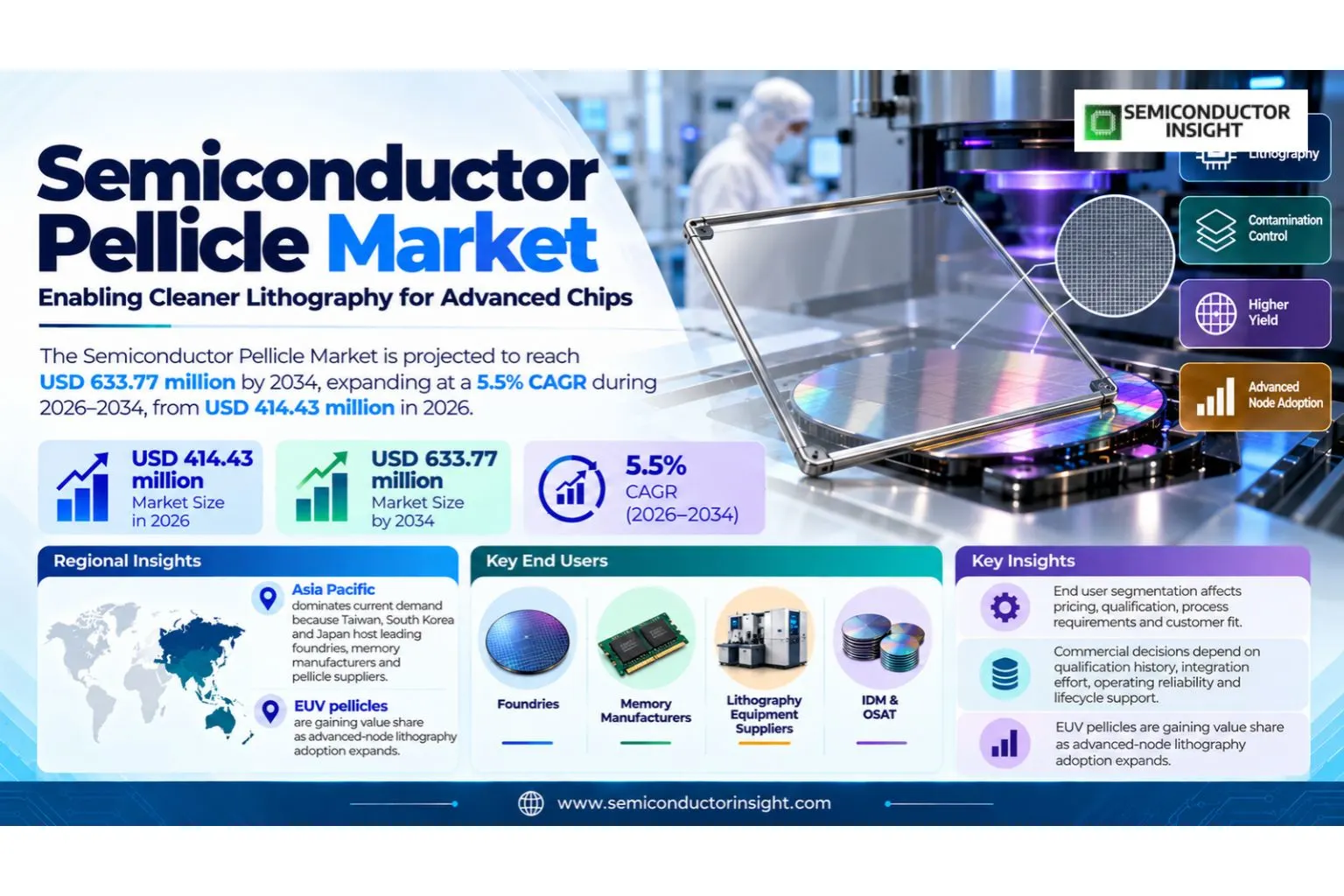
Semiconductor pellicle market is valued at USD 393.00 million in 2025 and is projected to reach USD 633.77 million by 2034, expanding at a 5.5% CAGR during 2026–2034. The 2026 market level is USD 414.43 million. Asia Pacific dominates current demand because Taiwan, South Korea and Japan host leading foundries, memory manufacturers and pellicle suppliers. EUV pellicles are gaining value share as advanced-node lithography adoption expands.
Semiconductor Pellicle products provide a critical functional layer inside modern electronic and industrial systems. Their commercial value depends on performance, reliability, manufacturability, qualification and compatibility with the broader hardware architecture. Customers increasingly assess total system impact rather than component price alone, which favors suppliers that combine proven technology with consistent global support.
Technology development is focused on euv membrane durability, higher optical transmission and advanced thin-film deposition, tighter integration and more automated manufacturing. These trends raise the value of precision process control and application engineering because smaller geometries, higher data rates or greater power density leave less margin for variation. Qualification therefore becomes a major barrier to entry in premium applications.
Commercial competition combines scale with specialization. Large suppliers benefit from purchasing power, engineering resources and global manufacturing, while specialist vendors can win through process expertise or application-specific performance. Design wins are often durable because changing suppliers can require requalification of electrical, thermal, mechanical or reliability performance. Commercial decisions in the Semiconductor Pellicle market also depend on qualification history, integration effort, operating reliability, lifecycle support and measurable system-level value.
Segment Analysis: By Type
By type, the market is segmented into ArF Pellicle, KrF Pellicle, EUV Pellicle, Others. Product selection depends on performance, cost, manufacturing complexity and the target system architecture. Higher-value variants generally offer tighter tolerances, greater integration or improved reliability, while mainstream categories retain volume leadership because of lower cost and broad compatibility.
| Type | Commercial role |
|---|---|
| ArF Pellicle | ArF Pellicle serves a distinct portion of the Semiconductor Pellicle market based on performance, cost and integration requirements. |
| KrF Pellicle | KrF Pellicle serves a distinct portion of the Semiconductor Pellicle market based on performance, cost and integration requirements. |
| EUV Pellicle | EUV Pellicle serves a distinct portion of the Semiconductor Pellicle market based on performance, cost and integration requirements. |
| Others | Others serves a distinct portion of the Semiconductor Pellicle market based on performance, cost and integration requirements. |
Additional Segmentation: By End User
End User segmentation highlights important technical or commercial differences inside the Semiconductor Pellicle market. These categories affect pricing, qualification, process requirements and customer fit, making them useful for evaluating where value growth differs from simple unit growth. Commercial decisions in the Semiconductor Pellicle market also depend on qualification history, integration effort, operating reliability, lifecycle support and measurable system-level value.
| End User | Demand characteristics |
|---|---|
| IDM | Integrated logic, memory and specialty semiconductor manufacturers. |
| Foundries | High-volume advanced-node lithography users requiring tight contamination control. |
| OSAT | Selected lithography and bumping processes in advanced packaging. |
Segment Analysis: By Application
By application, the market covers IC Foundry, IC Bumping, IC Substrate, MEMS, LED Package. Demand varies by reliability, performance and product lifecycle. Premium applications usually require stricter qualification and long-term supply support, while higher-volume applications place more emphasis on cost, manufacturing scale and rapid technology migration. Commercial decisions in the Semiconductor Pellicle market also depend on qualification history, integration effort, operating reliability, lifecycle support and measurable system-level value.
| Application | Demand characteristics |
|---|---|
| IC Foundry | IC Foundry is a material demand segment where reliability, cost and system performance influence purchasing decisions. |
| IC Bumping | IC Bumping is a material demand segment where reliability, cost and system performance influence purchasing decisions. |
| IC Substrate | IC Substrate is a material demand segment where reliability, cost and system performance influence purchasing decisions. |
| MEMS | MEMS is a material demand segment where reliability, cost and system performance influence purchasing decisions. |
| LED Package | LED Package is a material demand segment where reliability, cost and system performance influence purchasing decisions. |
Additional Segmentation: By Deposition Method
Deposition Method provides a second analytical view of the Semiconductor Pellicle market. It captures how product architecture and end-use requirements change supplier economics, qualification effort and technology roadmaps across the forecast period. Commercial decisions in the Semiconductor Pellicle market also depend on qualification history, integration effort, operating reliability, lifecycle support and measurable system-level value.
| Deposition Method | Commercial relevance |
|---|---|
| PVD | Physical-vapor-deposited films for selected pellicle structures. |
| CVD | Uniform thin-film deposition for advanced pellicle membranes and coatings. |
| Hybrid Methods | Multi-step deposition and reinforcement approaches for EUV and specialty pellicles. |
Regional Analysis
Asia Pacific is the largest regional market, while Asia Pacific is the fastest-growth region. Regional positioning reflects manufacturing concentration, downstream electronics demand, capital investment and the availability of qualified suppliers. Commercial decisions in the Semiconductor Pellicle market also depend on qualification history, integration effort, operating reliability, lifecycle support and measurable system-level value.
Why does regional demand differ across the Semiconductor Pellicle market?
Regional demand varies with electronics manufacturing, technology adoption and local investment. Asia Pacific combines the world’s largest advanced semiconductor manufacturing base with leading lithography material suppliers, while North America and Europe remain important through leading-edge logic R&D and EUV tool ecosystems. Commercial decisions in the Semiconductor Pellicle market also depend on qualification history, integration effort, operating reliability, lifecycle support and measurable system-level value.
| Region | Position | Demand profile | Supplier-selection factor |
|---|---|---|---|
| Asia Pacific | Largest / strategic | Technology and end-market demand | Qualification, cost and local support |
| North America | Strategic | Technology and end-market demand | Qualification, cost and local support |
| Europe | Strategic | Technology and end-market demand | Qualification, cost and local support |
| South America | Strategic | Technology and end-market demand | Qualification, cost and local support |
| Middle East & Africa | Strategic | Technology and end-market demand | Qualification, cost and local support |
Competitive Landscape
Mitsui Chemicals, Shin-Etsu Chemical, FINE SEMITECH, S&S Tech and advanced lithography-material suppliers form the core competitive landscape. Suppliers differentiate through process capability, product breadth, qualification history, manufacturing scale and technical support. Commercial decisions in the Semiconductor Pellicle market also depend on qualification history, integration effort, operating reliability, lifecycle support and measurable system-level value.
The competitive frontier is shifting toward euv membrane durability, higher optical transmission and advanced thin-film deposition, which raises the value of engineering integration and reduces the importance of price alone in premium segments. Commercial decisions in the Semiconductor Pellicle market also depend on qualification history, integration effort, operating reliability, lifecycle support and measurable system-level value.
Customer relationships are durable because qualified products become embedded inside longer-lived systems. This creates switching costs but also requires suppliers to maintain lifecycle support and predictable quality. Commercial decisions in the Semiconductor Pellicle market also depend on qualification history, integration effort, operating reliability, lifecycle support and measurable system-level value. Buyers therefore evaluate technical performance together with manufacturability, supply continuity and the cost of maintaining the solution across its intended service life.
| Competitive tier | Representative companies | Primary differentiation |
|---|---|---|
| Global leaders | Mitsui Chemicals, Shin-Etsu Chemical, FINE SEMITECH, S&S Tech and advanced lithography-material suppliers | Scale, technology and customer qualification. |
| Specialists | Regional and application-focused vendors | Process expertise and niche performance. |
| Emerging suppliers | New regional entrants | Cost, local capacity and diversification. |
Key companies profiled
Mitsui Chemicals, Shin-Etsu Chemical, FINE SEMITECH, S&S Tech and advanced lithography-material suppliers are included in the competitive scope. Their positions differ by product mix, technology capability, geographic manufacturing footprint and customer qualification. Commercial decisions in the Semiconductor Pellicle market also depend on qualification history, integration effort, operating reliability, lifecycle support and measurable system-level value.
Production Capacity Analysis
Capacity depends on specialized materials, precision manufacturing, automated inspection and qualified final test. Effective output is determined by saleable yield and customer-approved capacity rather than nominal equipment throughput alone. Commercial decisions in the Semiconductor Pellicle market also depend on qualification history, integration effort, operating reliability, lifecycle support and measurable system-level value.
Supply expansion increasingly requires duplicated qualification across several factories. This is strategically important because customers want resilience without sacrificing consistency, particularly in automotive, data-center, industrial and high-reliability applications. Commercial decisions in the Semiconductor Pellicle market also depend on qualification history, integration effort, operating reliability, lifecycle support and measurable system-level value.
Market Dynamics
The market is driven by electronics content growth, system performance requirements and supply-chain modernization. Growth is restrained by capital intensity, qualification cycles and pricing pressure. EUV membrane durability, higher optical transmission and advanced thin-film deposition creates the strongest opportunity for premium value growth. Commercial decisions in the Semiconductor Pellicle market also depend on qualification history, integration effort, operating reliability, lifecycle support and measurable system-level value.
Market Drivers
| Driver | Impact | Commercial mechanism |
|---|---|---|
| Technology migration | High | EUV membrane durability, higher optical transmission and advanced thin-film deposition increases product value and complexity. |
| Electronics demand | High | More electronic content increases component consumption. |
| Supply diversification | Medium-High | Customers want qualified capacity across several regions. |
| Automation | Medium | Higher automation improves yield and throughput. |
Technology migration
Customers are adopting more advanced architectures to improve performance, density or efficiency. This raises qualification and process-control requirements and supports premium pricing for technically differentiated suppliers. Commercial decisions in the Semiconductor Pellicle market also depend on qualification history, integration effort, operating reliability, lifecycle support and measurable system-level value. Buyers therefore evaluate technical performance together with manufacturability, supply continuity and the cost of maintaining the solution across its intended service life.
Electronics demand
Growth in automotive, data centers, industrial automation and connected devices expands the installed base requiring Semiconductor Pellicle products. Commercial decisions in the Semiconductor Pellicle market also depend on qualification history, integration effort, operating reliability, lifecycle support and measurable system-level value. Buyers therefore evaluate technical performance together with manufacturability, supply continuity and the cost of maintaining the solution across its intended service life.
Supply diversification
Geopolitical and logistics risk encourage multi-site sourcing, creating opportunities for suppliers that can replicate quality across factories. Commercial decisions in the Semiconductor Pellicle market also depend on qualification history, integration effort, operating reliability, lifecycle support and measurable system-level value. Buyers therefore evaluate technical performance together with manufacturability, supply continuity and the cost of maintaining the solution across its intended service life.
Automation
Automated process control, inspection and material handling can reduce variation and support larger production volumes. Commercial decisions in the Semiconductor Pellicle market also depend on qualification history, integration effort, operating reliability, lifecycle support and measurable system-level value. Buyers therefore evaluate technical performance together with manufacturability, supply continuity and the cost of maintaining the solution across its intended service life.
Market Restraints
| Restraint | Impact | Commercial consequence |
|---|---|---|
| Capital intensity | High | Advanced manufacturing requires specialized equipment. |
| Qualification cycles | Medium-High | Customer approval can take many months. |
| Price pressure | Medium | High-volume segments face continuing cost reduction. |
| Supply-chain risk | Medium | Specialized materials or equipment can be concentrated. |
Capital intensity
New Semiconductor Pellicle capacity can require significant equipment and qualification investment before revenue scales. Commercial decisions in the Semiconductor Pellicle market also depend on qualification history, integration effort, operating reliability, lifecycle support and measurable system-level value. Buyers therefore evaluate technical performance together with manufacturability, supply continuity and the cost of maintaining the solution across its intended service life.
Qualification cycles
Reliability validation and system integration slow supplier switching and delay new-factory ramps. Commercial decisions in the Semiconductor Pellicle market also depend on qualification history, integration effort, operating reliability, lifecycle support and measurable system-level value. Buyers therefore evaluate technical performance together with manufacturability, supply continuity and the cost of maintaining the solution across its intended service life.
Price pressure
Suppliers must offset lower average selling prices with yield, automation and differentiated technology. Commercial decisions in the Semiconductor Pellicle market also depend on qualification history, integration effort, operating reliability, lifecycle support and measurable system-level value. Buyers therefore evaluate technical performance together with manufacturability, supply continuity and the cost of maintaining the solution across its intended service life.
Supply-chain risk
Dependence on limited upstream suppliers can affect lead times and create the need for strategic inventory or second sourcing. Commercial decisions in the Semiconductor Pellicle market also depend on qualification history, integration effort, operating reliability, lifecycle support and measurable system-level value. Buyers therefore evaluate technical performance together with manufacturability, supply continuity and the cost of maintaining the solution across its intended service life.
Market Opportunities
EUV membrane durability, higher optical transmission and advanced thin-film deposition
EUV membrane durability, higher optical transmission and advanced thin-film deposition can expand value per unit and improve system performance. Commercial decisions in the Semiconductor Pellicle market also depend on qualification history, integration effort, operating reliability, lifecycle support and measurable system-level value. Buyers therefore evaluate technical performance together with manufacturability, supply continuity and the cost of maintaining the solution across its intended service life.
Regional manufacturing
New qualified capacity can support customers seeking geographic diversification. Commercial decisions in the Semiconductor Pellicle market also depend on qualification history, integration effort, operating reliability, lifecycle support and measurable system-level value. Buyers therefore evaluate technical performance together with manufacturability, supply continuity and the cost of maintaining the solution across its intended service life.
Automation and inspection
Better process control can raise yield and reduce lifecycle cost. Commercial decisions in the Semiconductor Pellicle market also depend on qualification history, integration effort, operating reliability, lifecycle support and measurable system-level value. Buyers therefore evaluate technical performance together with manufacturability, supply continuity and the cost of maintaining the solution across its intended service life.
Application-specific products
Tailored designs can capture premium niches with stronger qualification barriers. Commercial decisions in the Semiconductor Pellicle market also depend on qualification history, integration effort, operating reliability, lifecycle support and measurable system-level value. Buyers therefore evaluate technical performance together with manufacturability, supply continuity and the cost of maintaining the solution across its intended service life.
Supply Chain Analysis
Upstream. Specialized materials, wafers, laminates, metals or process equipment provide the technical foundation. Quality at this stage influences downstream yield and reliability. Commercial decisions in the Semiconductor Pellicle market also depend on qualification history, integration effort, operating reliability, lifecycle support and measurable system-level value. Buyers therefore evaluate technical performance together with manufacturability, supply continuity and the cost of maintaining the solution across its intended service life.
Manufacturing. Suppliers use precision process control and automated inspection to produce Semiconductor Pellicle products within tight tolerances. Yield improvement is a major economic lever. Commercial decisions in the Semiconductor Pellicle market also depend on qualification history, integration effort, operating reliability, lifecycle support and measurable system-level value. Buyers therefore evaluate technical performance together with manufacturability, supply continuity and the cost of maintaining the solution across its intended service life.
Integration. Products are qualified inside customer systems where electrical, thermal or mechanical behavior is validated. Design changes can trigger additional testing. Commercial decisions in the Semiconductor Pellicle market also depend on qualification history, integration effort, operating reliability, lifecycle support and measurable system-level value. Buyers therefore evaluate technical performance together with manufacturability, supply continuity and the cost of maintaining the solution across its intended service life.
Deployment. Finished products enter electronics, industrial, automotive, data-center or aerospace systems. Lifecycle support and supply continuity determine long-term customer value. Commercial decisions in the Semiconductor Pellicle market also depend on qualification history, integration effort, operating reliability, lifecycle support and measurable system-level value. Buyers therefore evaluate technical performance together with manufacturability, supply continuity and the cost of maintaining the solution across its intended service life.
Recent Developments in the Semiconductor Pellicle Market
Developments tracked through September 2026 and limited to events that materially affect technology, capacity, adoption or competition.
- 2026 EUV Lithography
ASML continues advancing EUV lithography systems and ecosystem requirements, increasing the importance of contamination control and thermally stable pellicles at leading nodes. Source - 2026 Pellicle Materials
Shin-Etsu continues supplying pellicles for semiconductor photomasks across advanced lithography applications. Source - 2026 Advanced Nodes
Continued EUV adoption across logic and memory increases technical requirements for pellicle transmission, durability and defect control. Source
Report Scope & Segmentation
| Attribute | Scope |
|---|---|
| Base year | 2025 |
| Estimated year | 2026 |
| Forecast period | 2026–2034 |
| 2025 market size | USD 393.00 million |
| 2026 estimated size | USD 414.43 million |
| 2034 projected size | USD 633.77 million |
| CAGR (2026–2034) | 5.5% |
| Largest market in 2025 | Asia Pacific |
| By Type | ArF Pellicle; KrF Pellicle; EUV Pellicle; Others |
| By Application | IC Foundry; IC Bumping; IC Substrate; MEMS; LED Package |
| By End User | IDM; Foundries; OSAT |
| By Deposition Method | PVD; CVD; Hybrid Methods |
| Companies profiled | Mitsui Chemicals, Shin-Etsu Chemical, FINE SEMITECH, S&S Tech and advanced lithography-material suppliers |
Frequently Asked Questions
What is the Semiconductor Pellicle market size in 2025?
The global market is valued at USD 393.00 million in 2025.
What is the market forecast for 2034?
The market is projected to reach USD 633.77 million by 2034, representing a 5.5% CAGR during 2026–2034. The 2026 market level is USD 414.43 million.
Which region leads the market?
Asia Pacific is the largest market, while Asia Pacific has the strongest growth profile.
Which type is most important?
ArF Pellicle is a leading category within the current market structure.
Which applications matter most?
IC Foundry and other listed applications are the principal demand segments.
What technology trend matters most?
EUV membrane durability, higher optical transmission and advanced thin-film deposition is a major technology and competitive trend.
Who are the major suppliers?
Major participants include Mitsui Chemicals, Shin-Etsu Chemical, FINE SEMITECH, S&S Tech and advanced lithography-material suppliers.
What drives market growth?
Electronics content, technology upgrades, automation and supply-chain modernization are the main growth drivers.
What limits growth?
Capital intensity, qualification cycles, price pressure and supply-chain concentration are the main restraints.
What will shape the market through 2034?
EUV membrane durability, higher optical transmission and advanced thin-film deposition, regional manufacturing diversification and more automated production will shape the market through 2034.
Research Sources & Evidence Base
View research sources used in this market overview
- ASML — EUV Lithography. Current EUV lithography and advanced-node ecosystem context.
- Shin-Etsu Chemical — Pellicles. Current semiconductor pellicle product and application context.
Get Sample Report PDF for Exclusive Insights
Report Sample Includes
- Table of Contents
- List of Tables & Figures
- Charts, Research Methodology, and more...
 Download Sample Report PDF