Semiconductor Package Probe Market Insights
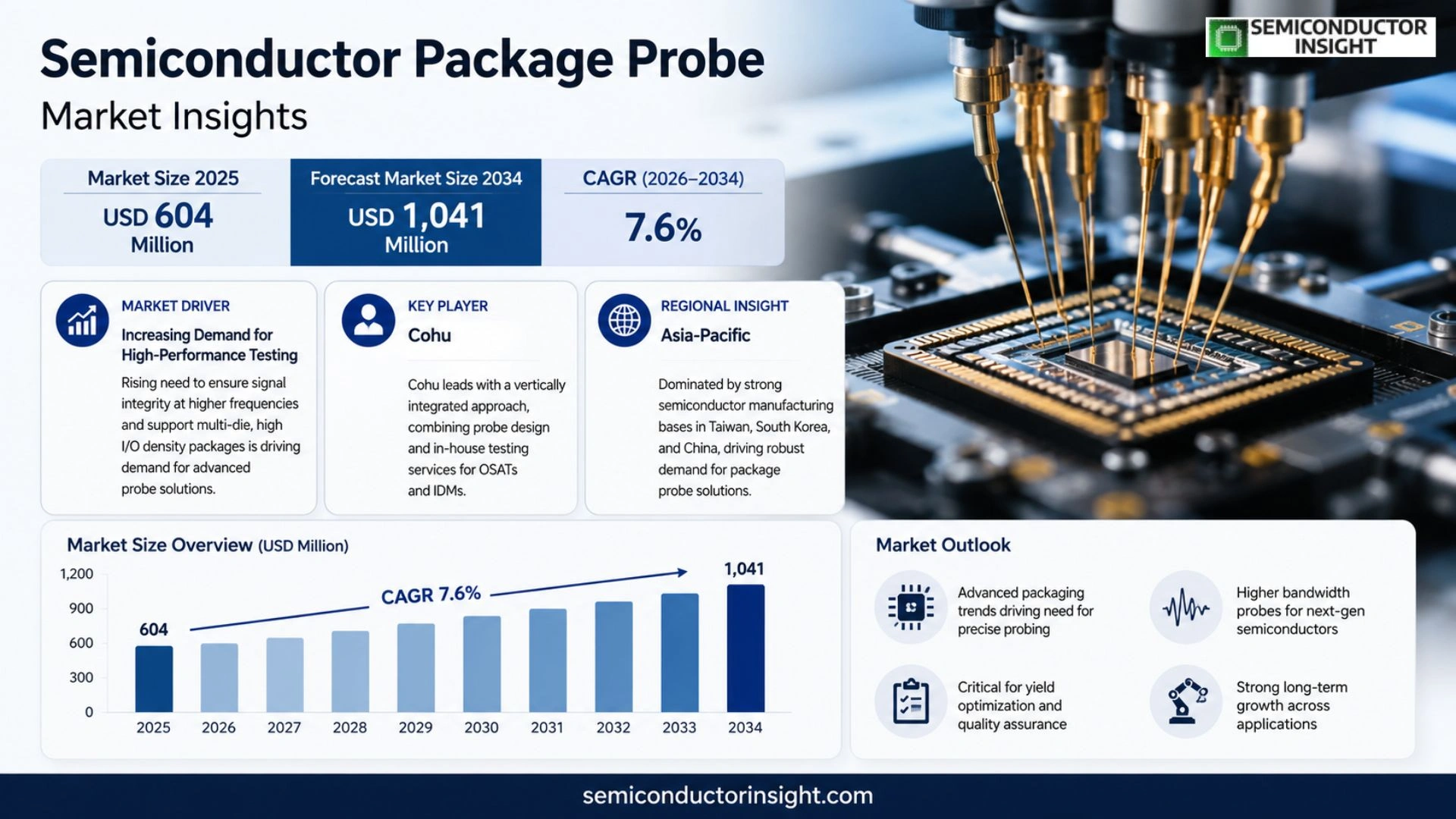
Semiconductor Package Probe market was valued at USD 604 million in 2025 and reached an estimated USD 1,041 million by 2034, indicating an implied compound annual growth rate of approximately 7.6 percent over the nine‑year horizon.
Semiconductor Package Probes are precision contact components employed during package‑level or final testing; they create temporary electrical links between test equipment and devices such as BGA, CSP, QFN, LGA and SiP, enabling verification of performance, functionality and reliability before shipment. In 2025 global production reached roughly 710 million units at an average price of about USD 932 per thousand units, while capacity stood near 750 million units. The typical gross margin ranges from 20 to 40 percent, reflecting their status as high‑value consumables for OSATs and IDMs.
MARKET DRIVERS
Increasing Demand for High‑Performance Testing
Semiconductor Package Probe Market is being pulled forward by manufacturers that must verify signal integrity at ever‑higher frequencies. As silicon architectures shift toward multi‑die and heterogeneous integration, test engineers require probes that can access densely packed I/O without compromising electrical performance. This pressure translates into a steady stream of orders for advanced probe assemblies that support finer pitch and broader bandwidth.
Advancements in Miniaturization Technology
Progress in lithography and package‑on‑package designs has driven the probe industry toward sub‑micron tip dimensions. Suppliers that can deliver probes with reduced parasitic capacitance enable chip makers to push the envelope of power efficiency. Consequently, firms that invest in precision micro‑fabrication are gaining a competitive edge, prompting a re‑allocation of R&D budgets toward probe‑centric capabilities.
➤ Customers prioritize probe solutions that minimize signal distortion while surviving aggressive thermal cycles, making reliability a decisive purchasing factor.
Beyond pure technical merits, the shift toward automated test equipment (ATE) platforms that support parallel probing creates volume opportunities. OEMs that align their probe portfolios with the modular architecture of modern ATE can capture incremental market share through bundled offerings.
MARKET CHALLENGES
Complexity of Probe Design
Designing probes that accommodate both ultra‑fine pitch and high‑frequency operation demands sophisticated simulation tools and multi‑material stacks. Many midsize vendors lack the depth of expertise to iterate quickly, leading to longer lead times and higher engineering costs. This complexity can deter smaller foundries from adopting the latest probe generations.
Other Challenges
Cost Pressures
The capital intensity of precision probe manufacturing, combined with price sensitivity among downstream testers, squeezes margins. Companies must balance the need for cutting‑edge performance with the imperative to keep unit costs competitive, often resulting in trade‑offs that affect yield.
MARKET RESTRAINTS
Stringent Reliability Standards
Regulatory bodies and end‑user specifications impose tight reliability thresholds for probe wear, especially in automotive and aerospace applications. Meeting these standards requires extensive qualification cycles, which can delay product launches and increase upfront investment. Suppliers that cannot demonstrate compliance risk exclusion from high‑value contracts.
MARKET OPPORTUNITIES
Emerging Applications in 5G Infrastructure
The rollout of 5G networks introduces a new set of testing requirements for RF front‑ends and millimeter‑wave modules. Probes capable of handling frequencies above 30 GHz are in short supply, presenting an opening for firms that can engineer high‑frequency, low‑loss solutions. Capturing this niche could add a meaningful revenue stream to Semiconductor Package Probe Market as telecom vendors accelerate production cycles.
Semiconductor Package Probe Market Trends
Advanced Packaging Fuels Probe Innovation
The surge in heterogeneous integration and high‑pin‑count devices has reshaped the testing landscape. As chip architectures incorporate finer pitches and stacked dies, the need for probes that preserve signal fidelity while contacting dense arrays intensifies. Manufacturers are therefore investing in materials that reduce wear and enhance acoustic impedance, allowing test cycles to stay short without compromising yield. This technical shift, observed across logic, memory and power segments, translates into higher unit prices that still sit below the $1,000 mark per probe, preserving the market’s profit envelope of 20‑40 %.
Other Trends
Durability Requirements from AI and Automotive Segments
AI accelerators and automotive electronics demand probes that survive thousands of insertion cycles while maintaining low insertion loss. The rise of silicon‑photonic interposers and SiP modules forces suppliers to optimize tip geometry,particularly conical and crown designs,so that contact pressure distributes evenly across solder balls. Companies that can certify longer probe lifespans gain a bargaining edge with OSATs, which value reduced inventory turnover and lower downtime during final‑package verification.
Customization and Qualification Lead Times
Qualification remains a lengthy, customer‑specific process because each new package design often mandates a unique probe configuration. Consequently, firms with flexible manufacturing cells and rapid prototyping capabilities capture premium projects that others cannot service within acceptable lead times. This environment encourages consolidation among players possessing advanced precision machining, while niche specialists focus on niche tip‑shape variations to address emerging high‑frequency test demands.
COMPETITIVE LANDSCAPE
Key Industry Players
Semiconductor Package Probe Market – Competitive Overview
Among the handful of firms that dominate the probe‑manufacturing supply chain, Cohu stands out for its vertically integrated model that couples probe design with in‑house testing services for OSATs and IDMs. This breadth allows Cohu to command a sizable share of the $1.0 billion market projected for 2032, while its precision‑cantilever portfolio meets the high‑frequency demands of AI‑chip testing. The company’s ability to scale production to the 750 million‑unit capacity noted in 2025, coupled with gross margins hovering between 20 % and 40 %, reinforces a defensible position that smaller suppliers find difficult to replicate. Cohu’s strategy of locking in long‑term qualification contracts reduces customer churn and creates a quasi‑subscription revenue stream that smooths the inherent volatility of test‑equipment cycles.
Beyond the market leader, a cadre of niche specialists adds depth to the competitive map. LEENO and QA Technology have carved out profitable segments around flexible and vertical probes, leveraging proprietary tip‑geometry patents that improve signal integrity for high‑pin‑count packages. Meanwhile, Smiths Interconnect and Yokowo Co., Ltd. differentiate through material science expertise, supplying conical and crown‑shaped probes that survive extreme automotive‑grade thermal cycles. Smaller innovators such as Feinmetall, Qualmax, and PTR HARTMANN (Phoenix Mecano) focus on customized solutions for emerging SiP applications, often partnering directly with semiconductor fabless firms to accelerate time‑to‑market. This fragmented yet highly specialized landscape forces incumbents to pursue both organic R&D and selective acquisitions to preserve relevance in a market where test complexity continues to rise.
List of Key Semiconductor Package Probe Companies Profiled
- Cohu
- LEENO
- QA Technology
- Smiths Interconnect
- Yokowo Co., Ltd.
- INGUN
- Feinmetall
- Qualmax
- PTR HARTMANN (Phoenix Mecano)
- Seiken Co., Ltd.
- TESPRO
- AIKOSHA
- CCP Contact Probes
- Da‑Chung
- UIGreen
Segment Analysis:
| Segment Category | Sub-Segments | Key Insights |
| By Type |
|
Flexible Probe
|
| By Application |
|
Packaging and Testing
|
| By End User |
|
OSATs
|
Regional Analysis: Semiconductor Package Probe Market
Asia‑Pacific
The bulk of probe wafer processing is clustered in the Taiwan–South Korea corridor, where fab capacity aligns with the high‑density interconnect needs of leading chipmakers. Proximity to front‑end fabs reduces die‑handling cycles, enabling tighter schedule adherence and lower logistics costs for customers across the value chain. This geographical advantage also supports rapid feedback loops between probe designers and device engineers, accelerating qualification cycles.
University‑linked research centers in Singapore and Japan are feeding the probe market with novel materials such as high‑k dielectrics and flexible substrates. Collaborative programs between academia and corporate R&D labs accelerate proof‑of‑concept projects, translating into faster deployment of probes compatible with emerging 3‑D stacking and chip‑on‑wafer technologies. These efforts often culminate in intellectual‑property filings that reinforce the region’s strategic positioning.
Recent disruptions have prompted manufacturers to diversify component sourcing, yet many still rely on a tightly woven network of substrate suppliers, precision aligners, and metrology firms located within the same industrial clusters. This interdependence creates a buffer against global shortages, as alternate lines can be activated without extensive re‑qualification. The ability to shift workloads across nearby fabs minimizes downtime and preserves market share for probe producers.
Governments across the region have introduced subsidies and tax reliefs specifically targeting advanced test equipment, including high‑frequency probes. While standards bodies in Japan and South Korea enforce stringent quality criteria, the overall regulatory environment encourages rapid certification, allowing companies to bring new probe families to market within compressed timeframes. Compliance costs remain modest compared with North America, making the region attractive for firms seeking cost‑effective development cycles.
North America
North America retains a sophisticated customer base for Semiconductor Package Probe Market, driven by leading design houses and a mature ecosystem of test service providers. The United States’ emphasis on high‑performance computing and automotive electronics sustains demand for probes capable of supporting fine‑pitch interconnects and elevated data rates. However, the region grapples with higher labor costs and a fragmented supply chain that often necessitates imports from Asia‑Pacific to meet volume requirements. Recent policy initiatives aim to repatriate certain segments of probe manufacturing through incentives for domestic fab upgrades, yet the timeline for achieving parity with Asian producers remains extended. Consequently, North American players are focusing on value‑added services such as probe‑performance analytics and customized test‑fixture integration to differentiate themselves.
Europe
Europe’s semiconductor landscape, centered around Germany, the Netherlands, and the United Kingdom, places a premium on precision and reliability, traits that shape the regional Semiconductor Package Probe Market. The region’s automotive and industrial automation sectors demand probes that can endure harsh operating conditions while delivering consistent signal integrity. A notable trend is the collaboration between equipment manufacturers and research institutes to develop probes aligned with emerging EU standards on energy efficiency. Supply constraints compel many European firms to maintain strategic inventories sourced from Asia‑Pacific, creating a hybrid procurement model. To offset cost pressure, European companies are leveraging advanced simulation tools and modular probe architectures that enable rapid adaptation to new package formats.
South America
South America exhibits a modest yet evolving presence in Semiconductor Package Probe Market, with Brazil leading regional activity due to its growing consumer electronics assembly sector. Local OEMs prioritize cost‑effective probing solutions that can support midsize production runs without excessive capital outlay. Limited domestic component manufacturers result in a reliance on imported probes, which raises lead times and introduces currency‑related price volatility. Recent governmental programs aim to attract foreign investment in test facilities, hoping to establish a regional hub that can serve both local and neighboring Latin American markets. In the short term, the market’s growth will hinge on the ability of distributors to provide responsive technical support and flexible payment structures.
Middle East & Africa
The Middle East & Africa region remains a nascent arena for Semiconductor Package Probe Market, with activities concentrated in United Arab Emirates and South Africa. The primary driver is the rise of data‑center projects and telecommunications upgrades that require reliable probe assemblies for server‑level testing. Infrastructure investments are prompting multinational test‑equipment vendors to open satellite service centers, offering localized calibration and spare‑part logistics. Skilled labor shortages and limited local manufacturing capacity mean most probes are imported, yet the region’s strategic positioning along major shipping lanes reduces transit delays. As digital transformation initiatives accelerate, demand for high‑performance probes is expected to grow incrementally, encouraging suppliers to forge partnerships with regional system integrators.
Report Scope
This market research report provides a comprehensive analysis of the Semiconductor Package Probe Market , covering the forecast period 2026–2034. It offers detailed insights into market dynamics, technological advancements, competitive landscape, and key trends shaping the industry.
Key focus areas of the report include:
- Market Overview: The report begins with an overview outlining its current market scenario, key growth indicators, and industry transformation drivers. It discusses macroeconomic factors, demand–supply balance, regulatory landscape, and the strategic role of semiconductors in powering advancements across industries such as automotive, telecommunications, consumer electronics, and industrial automation.
- Market Size & Forecast: Historical data and future projections for revenue, unit shipments, and market value across major regions and segments.
- Segmentation Analysis: Detailed breakdown by product type, technology, application, and end-user industry to identify high-growth segments and investment opportunities.
- Regional Insights: Insights into market performance across North America, Europe, Asia-Pacific, Latin America, and the Middle East & Africa, including country-level analysis where relevant.
- Competitive Landscape: Profiles of leading market participants, including their product offerings, R&D focus, manufacturing capacity, pricing strategies, and recent developments such as mergers, acquisitions, and partnerships.
- Technology Trends & Innovation: Assessment of emerging technologies, integration of AI/IoT, semiconductor design trends, fabrication techniques, and evolving industry standards.
- Market Drivers & Restraints: Evaluation of factors driving market growth along with challenges, supply chain constraints, regulatory issues, and market-entry barriers.
- Stakeholder Insights: Insights for component suppliers, OEMs, system integrators, investors, and policymakers regarding the evolving ecosystem and strategic opportunities.
Primary and secondary research methods are employed, including interviews with industry experts, data from verified sources, and real-time market intelligence to ensure the accuracy and reliability of the insights presented.
FREQUENTLY ASKED QUESTIONS:
What is the current market size of Semiconductor Package Probe Market?
-> Semiconductor Package Probe Market was valued at USD 604 million in 2025 and is expected to reach USD 1,041 million by 2032 with a CAGR of 7.6% during the forecast period.
Which key companies operate in Semiconductor Package Probe Market?
-> Key players include LEENO, Cohu, QA Technology, Smiths Interconnect, Yokowo Co., Ltd., INGUN, Feinmetall, Qualmax, PTR HARTMANN (Phoenix Mecano), Seiken Co., Ltd., TESPRO, AIKOSHA, CCP Contact Probes, Da-Chung, UIGreen, Centalic, Woodking Tech, Lanyi Electronic, Merryprobe Electronic, Tough Tech, Hua Rong.
What are the key growth drivers?
-> Key growth drivers include increasing adoption of AI chips, expansion of automotive electronics, high‑reliability industrial applications, and the need for greater probe durability, signal integrity, and high‑parallel testing capability driven by advanced packaging and heterogeneous integration.
Which region dominates the market?
-> Asia dominates Semiconductor Package Probe market, driven by large manufacturing bases, high‑volume OSAT and IDM testing activities, and rapid growth in AI and automotive semiconductor demand.
What are the emerging trends?
-> Emerging trends include development of high‑pin‑count and high‑frequency probes, customization for heterogeneous integration, and the push toward higher test parallelism to support advanced package architectures.

Get Sample Report PDF for Exclusive Insights
Report Sample Includes
- Table of Contents
- List of Tables & Figures
- Charts, Research Methodology, and more...
 Download Sample Report PDF