Key Statistics
Key Takeaways
- USD 3,589 million in 2025 sets the starting point for a CMP ecosystem spanning slurry, pads, conditioners, point-of-use filtration, PVA brushes and retaining rings. The commercial requirement is not simply more polishing capacity; it is repeatable material removal with low defectivity across 200mm and 300mm wafers, which keeps consumables qualification closely tied to fab process integration and tool uptime.
- 300mm wafer processing is the center of demand, with advanced logic and memory fabs creating frequent polishing steps and tighter process windows. TSMC reported fourth-quarter 2025 revenue of USD 33.73 billion, with 3nm, 5nm and 7nm contributing 28%, 35% and 14% of revenue respectively, showing how much high-value wafer manufacturing is exposed to the planarization performance of qualified consumables.
- Advanced-metal slurry development is the strongest technology-growth axis as cobalt, molybdenum, tungsten, copper, barrier layers and front-end structures expand the number of material-specific polishing requirements. SEMI’s 2026 CMP program explicitly covers these materials and structures, while suppliers such as Fujifilm and Resonac emphasize selectivity, particle control and emerging-node compatibility, shifting competition toward process-specific formulations instead of commodity abrasive volume.
- Asia Pacific remains the largest regional market through its concentration of Taiwan, South Korea, Japan and China semiconductor production and materials supply. The regional advantage is reinforced by local qualification networks, short replenishment cycles and dense technical support. North America is the fastest-developing expansion market as TSMC, Intel and Micron add domestic leading-edge or memory capacity, creating new qualification sites for CMP suppliers.
- Competitive differentiation is increasingly systems-oriented. Slurry chemistry, pads, conditioners and filtration interact, so a supplier that can solve selectivity, defectivity, polishing rate and contamination control as one process package has more commercial leverage than a vendor selling a single consumable. Long-term agreements, co-development, application engineering and global logistics therefore become important barriers to substitution even when several suppliers can technically make an individual product.
Semiconductor Materials for CMP Market Overview
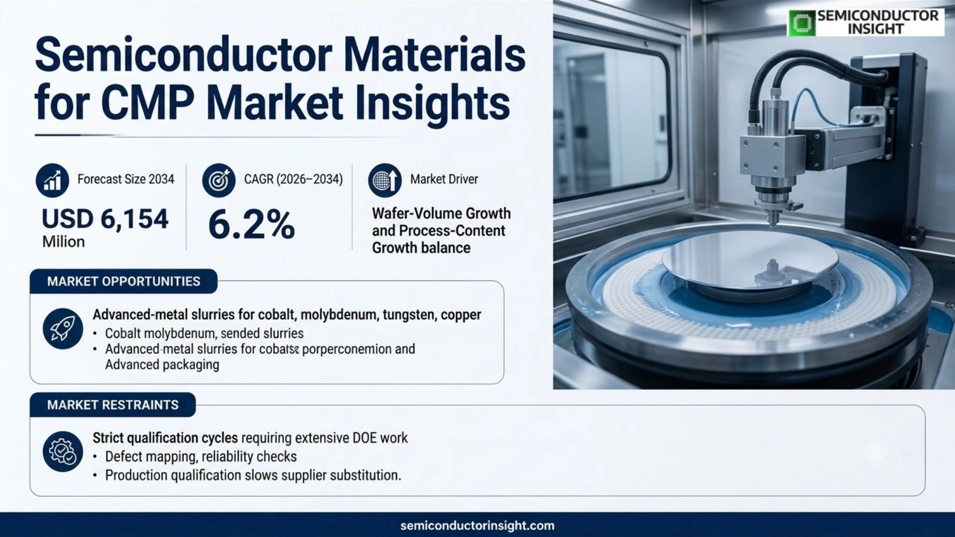
semiconductor materials for CMP market was valued at USD 3,380 million in 2024 and, reaches USD 3,589 million in 2025 and approximately USD 6,154 million in 2034, implying a 6.2% CAGR for 2026–2034. The market covers CMP slurry, pads, pad conditioners, point-of-use slurry filters, PVA brushes and retaining rings used to planarize or clean semiconductor wafer surfaces.
Chemical mechanical planarization is the process stage that turns a patterned wafer surface into a controlled, sufficiently flat structure for subsequent lithography, deposition, etch and interconnect operations. The materials package combines chemical removal with mechanical contact: slurry establishes the selective chemical environment, the pad supplies controlled contact, the conditioner maintains pad texture, the filter protects the slurry stream, and brushes and retaining rings support post-polish cleanliness and wafer positioning. Commercial value therefore comes from process repeatability, not merely consumption volume.
The technology stack becomes more demanding as device architectures add three-dimensional structures and new conductor or barrier materials. SEMI’s 2026 CMP technology program covers oxide, polysilicon, barrier, shallow-trench isolation, cobalt, copper, molybdenum and tungsten, while also addressing FinFET, gate-all-around, 3D NAND and other advanced structures. This expanding material set forces suppliers to tune removal rate, selectivity, surface roughness, defectivity and residue control together, which increases qualification work and strengthens the value of formulation know-how.
Demand follows the number of wafers processed, the number of planarization steps per wafer and the difficulty of the film stack being polished. SEMI reported global semiconductor-materials revenue of USD 73.2 billion in 2025, including USD 45.8 billion for wafer-fabrication materials, confirming the scale of the input market surrounding wafer processing. Within that ecosystem, CMP consumables are recurrently consumed and replenished, while qualification changes can take longer than a purchasing cycle. Suppliers therefore compete on technical support, global availability and process stability as much as on unit price.
The commercial landscape is also becoming geographically distributed. Leading wafer makers are expanding in Taiwan, Korea, Japan, China, the United States and Europe, so customers increasingly want local application engineering, controlled logistics and contingency supply. TSMC’s Arizona investment, Intel’s 18A manufacturing in Arizona, Micron’s U.S. memory projects and policy-backed European fab programs all expand the map of qualification and replenishment points. For CMP suppliers, a wider fab footprint creates more addressable sites but also raises the operational burden of maintaining identical chemistry and consumable performance across regions.
Segment Analysis: By Type
The source-defined type architecture contains six categories: CMP Slurry, CMP Pads, CMP Pad Conditioners, CMP POU Slurry Filters, CMP PVA Brushes and CMP Retaining Rings. CMP slurry is the economic center of the consumables stack, while the highest technology momentum is visible in process-specific slurry formulations and conditioning solutions for new materials and advanced-node structures. The categories are interdependent: polishing rate or defectivity cannot be optimized from the chemical, mechanical and filtration components independently, so customer qualification increasingly evaluates the complete consumables recipe.
| Type | Demand and technical logic | Commercial position |
|---|---|---|
| CMP Slurry | Chemical formulations combine abrasive particles, oxidants, complexants and pH control to selectively remove films while limiting defects. Fujifilm covers copper, barrier, cobalt, front-end and post-CMP systems, illustrating how one supply family stretches from interconnect planarization to emerging materials. The purchasing decision centers on removal rate, selectivity, defectivity, shelf life and compatibility with the customer’s exact process stack. | Largest and broadest process-content pool |
| CMP Pads | Polyurethane pads set the mechanical contact environment that controls wafer pressure distribution, slurry transport and removal uniformity. DuPont’s IC1000 family spans copper bulk, tungsten, shallow-trench isolation, oxide and buff applications, showing why pad specification is tied to the film being polished rather than treated as a generic consumable. Pad lifetime and conditioning frequency directly affect cost per wafer. | High recurring consumption with application-specific grades |
| CMP Pad Conditioners | Diamond conditioners maintain the pad surface by removing glazing and restoring asperity structure during repeated polishing cycles. Their commercial role grows with high-volume 200mm and 300mm production as pad behavior changes continuously during a run. Suppliers compete on diamond retention, conditioning uniformity, wear life and compatibility with increasingly low-defect front-end and advanced-packaging processes. | Strong technology momentum in high-throughput uniformity control |
| CMP POU Slurry Filters | Point-of-use slurry filtration protects the polishing process from oversized particles, agglomerates and foreign material that can translate into wafer defects. Entegris positions its Solaris family for CMP slurry filtration with ratings extending to 0.03 micrometre-scale retention. The segment sits at the intersection of consumables and contamination control, making filter integrity, flow stability and change-out logistics commercial priorities. | Specialty contamination-control layer |
| CMP PVA Brushes | Polyvinyl-alcohol brushes support post-polish cleaning by removing residual slurry and loosely attached particles from wafer surfaces. As device structures become more fragile and pattern density rises, the purchasing trigger shifts toward controlled particle removal without scratching or pattern collapse. Brush porosity, hardness, chemistry compatibility and reproducible cleaning performance create a specialized consumables niche within the wider CMP ecosystem. | Specialty post-CMP cleaning consumable |
| CMP Retaining Rings | Retaining rings define the wafer position and influence pressure distribution at the polishing interface, so their geometry and wear state can affect edge exclusion and process repeatability. They are exposed to aggressive slurries and mechanical loading, creating recurring replacement demand. Customers value material stability, dimensional control and predictable life, particularly where high wafer utilization makes unscheduled changeovers disproportionately costly. | Recurring mechanical interface component |
Which secondary consumable axis changes purchasing decisions most?
Slurry formulation is the secondary axis with the greatest ability to change the total CMP recipe economics, while filter pore size, pad hardness, conditioner design and brush characteristics determine whether that chemistry can run stably at production scale. Fujifilm highlights copper, barrier, cobalt, front-end and post-CMP slurry families, while Entegris positions point-of-use filtration around sub-micrometre particle retention. Together, these products show that qualification is increasingly process-stack specific, linking chemistry selection to contamination control, consumable lifetime and wafer-level yield.
Segment Analysis: By Application
The application axis comprises 300mm Wafers, 200mm Wafers and Others. The 300mm segment is the commercial anchor and the most important source of technology-driven growth, with advanced logic and memory fabs running high-value wafer starts through many polishing steps. The purchasing trigger is wafer throughput combined with tight process windows: fabs pay for consistent removal and low defectivity that protect the downstream lithography and deposition sequence, while 200mm and specialty users emphasize long-term compatibility and service continuity.
| Application | Demand characteristics and purchasing trigger |
|---|---|
| 300mm Wafers | The 300mm application is the principal demand center as leading-edge logic and high-volume memory manufacturing use 300mm substrates as the standard production platform. TSMC reported 2025 fourth-quarter revenue of USD 33.73 billion, with 3nm at 28%, 5nm at 35% and 7nm at 14%, demonstrating the scale of advanced-node processing that requires repeated planarization steps. Suppliers therefore prioritize qualification depth, consistency and global fab support. |
| 200mm Wafers | The 200mm application remains commercially important for mature-node logic, analog, power, MEMS and specialty devices, and SEMI’s materials outlook explicitly points to renewed growth across 200mm and 300mm activity. Purchasing triggers differ from leading-edge fabs: long product lifecycles, equipment longevity and maintenance continuity become central, so CMP vendors compete on recipe stability, retrofit compatibility, regional availability and service support over extended manufacturing programs. |
| Others | The ‘Others’ category captures smaller or specialized wafer formats and non-standard production environments where polishing is still required but annual volume is lower or equipment configurations differ from mainstream 200mm and 300mm fabs. These customers often value process flexibility and technical support more heavily than maximum consumable throughput. The commercial opportunity is narrower, yet specialized chemistry or pad designs can command attractive margins when qualification requirements are demanding. |
How do wafer diameter and process complexity interact?
The economic difference between 200mm and 300mm CMP demand is not only wafer area. A 300mm fab usually couples larger wafer throughput with advanced process integration, making small excursions in removal rate or defectivity expensive at a high output level. A 200mm facility can have longer product lifecycles and older tool generations, which puts emphasis on formula continuity, retrofit compatibility and supplier support. The result is a two-speed market: leading-edge fabs drive chemistry innovation while mature fabs sustain replacement and qualified legacy demand.
Regional Analysis
Asia Pacific is the largest regional market on the basis of wafer-fabrication concentration, while North America has the strongest near-term expansion momentum from announced leading-edge and memory capacity programs. Asia’s leadership is rooted in existing production density and short supply chains for semiconductor materials; North America’s growth is linked to localization and new fab qualification. Europe follows a strategic-resilience model, while South America and the Middle East & Africa remain smaller, more project-driven markets.
Where is CMP materials demand concentrated, and where is the growth pipeline strongest?
| Region | Current position | Growth mechanism | Supply-chain logic | Commercial implication |
|---|---|---|---|---|
| Asia Pacific | Asia Pacific is the largest demand center, with Taiwan, South Korea, Japan and China combining major wafer-fab clusters with deep semiconductor-materials supply. The region benefits from high 200mm and 300mm wafer activity and dense process-engineering networks, so local customers can qualify and replenish consumables through established channels while suppliers optimize manufacturing and technical service around multiple nearby fabs. | Growth follows advanced-node expansion, memory investment and mature-node capacity. The mix supports recurring slurry, pad and filtration consumption plus new formulations for cobalt, tungsten, copper and emerging structures. | Materials production, packaging, equipment and process engineering sit close together, allowing shorter logistics cycles and faster troubleshooting during recipe changes or yield excursions. | Suppliers should prioritize local application engineers, regional inventory, contamination-control capability and multi-fab qualification programs rather than treating each site as a standalone account. |
| North America | North America is the fastest-developing expansion market as new leading-edge and memory projects add fabrication capacity while existing fabs remain important customers. TSMC’s Arizona investment and Intel’s Arizona 18A manufacturing create demand for qualified consumables closer to U.S. fabs, while Micron’s U.S. memory program extends the opportunity across several future manufacturing sites. | The mechanism is localization of production. New fabs require approved consumable recipes from tool installation through production ramp, making qualification activity arrive before full wafer volume and creating a long runway for suppliers that enter early. | Regional supply is increasingly about resilience, technical response time and contingency inventory rather than low unit cost. Customers want consistent material performance across international sites with local support for process changes. | The commercial priority is to win qualification in new fabs, establish local inventory and preserve global product equivalence so the same formulation can be transferred between Asia and North America without restarting development from zero. |
| Europe | Europe is a smaller demand market but a strategic materials and equipment ecosystem with policy support for semiconductor capacity. European Commission programs have backed multiple semiconductor projects, including 300mm manufacturing initiatives, which provides a platform for incremental CMP demand even without East Asia’s overall wafer-volume scale. | Growth is project-led and tied to strategic manufacturing resilience, specialty devices and advanced-node support. Demand can therefore be lumpy, with qualification and facility milestones more important than broad consumer-electronics cycles. | European customers place high value on controlled material documentation, environmental compliance, stable logistics and collaboration with established equipment and chemical suppliers. | Suppliers should align with major fab projects early, build regional technical capability and demonstrate consistent qualification data across chemistry, pad and filtration packages rather than relying only on distributor coverage. |
| South America | South America remains a smaller market where research, specialty electronics, assembly activity and targeted semiconductor programs generate the main CMP opportunities. Large continuous wafer volumes are limited relative to Asia, so the demand profile is less about building a local consumables manufacturing hub and more about supplying qualified materials into specialized production or development environments. | Growth is tied to discrete projects and technology-transfer initiatives. Buyers prioritize flexible quantities, stable lead times and technical assistance for process development where local CMP expertise may be narrower than in established fab clusters. | Imported materials and regional distribution are central, which increases the importance of shelf-life management, packaging integrity and contingency planning for long replenishment routes. | A focused supplier can capture value by offering small-lot technical support, documented process conditions and reliable replenishment rather than duplicating the full manufacturing footprint used in high-volume regions. |
| Middle East & Africa | Middle East & Africa is an emerging market whose semiconductor opportunity is tied to ecosystem formation, investment incentives and new technology clusters. Abu Dhabi identifies semiconductors as a growth sector, but established high-volume wafer processing remains much smaller than Asia’s base, so current CMP demand is more strategic than volume-driven. | The growth mechanism is new capability creation. As clusters attract design, packaging, specialty manufacturing and potential fabrication projects, CMP suppliers can participate earlier in equipment selection, qualification planning and technical training than would be possible in a mature fab market. | The supply-chain requirement is resilient import access combined with local technical presence. Environmental, storage and logistics conditions can influence delivery reliability for chemistry and consumables. | Early entrants can build an advantage by partnering with fabs, research organizations and cluster developers, establishing training and application support before a large installed base creates entrenched incumbent relationships. |
Detailed Regional Blocks
Asia Pacific
Why does Asia Pacific lead CMP materials consumption?
Asia Pacific leads through wafer-fab density, high 300mm utilization and an integrated ecosystem of chemical, equipment, memory and foundry suppliers. Taiwan and South Korea anchor advanced logic and memory, Japan contributes deep materials and equipment capabilities, and China adds broadening mature-node capacity. The regional commercial logic is recurring production volume: once a CMP formulation is qualified, every wafer lot creates ongoing consumable demand across the polishing sequence.
| Country / subregion | Commercial role and evidence |
|---|---|
| Taiwan | Taiwan combines very high foundry intensity with an extensive semiconductor-materials ecosystem. TSMC’s 2025 fourth-quarter revenue was USD 33.73 billion, with 3nm, 5nm and 7nm accounting for 28%, 35% and 14%, respectively. That production mix supports repeated CMP steps for front-end and interconnect structures, so suppliers compete on qualified recipes, response time and global-to-local product consistency. |
| South Korea | South Korea combines major memory manufacturing with strong materials and equipment supply chains. SK hynix announced KRW 54 trillion of facility investment in 2026, including KRW 35.2 trillion for Yongin Y2 and KRW 19.1 trillion for Cheongju M17. The resulting production roadmap supports long-duration demand for polishing chemistry, pads and filtration as fabs progress from cleanroom construction to process qualification and volume output. |
| Japan | Japan has a distinctive role as both a manufacturing market and a materials technology center. Resonac and Fujifilm develop CMP chemistries spanning advanced films and semiconductor front-end applications, while Japan also hosts major semiconductor equipment manufacturing. Suppliers can therefore gain from a combined production-and-development ecosystem where new formulations can be tested, qualified and industrialized before wider deployment. |
| China | China contributes a large mature-node and expanding advanced-node manufacturing base, alongside a growing domestic semiconductor-materials industry. The commercial requirement is continuity at scale: fabs seek qualified CMP materials with predictable supply, while local suppliers expand process-specific capabilities. International vendors face stronger localization expectations, making technical service, regulatory readiness and reliable regional manufacturing increasingly important competitive factors. |
| Southeast Asia | Southeast Asia is developing as a complementary electronics and semiconductor manufacturing base, with packaging, assembly, specialty production and selected wafer-fab activities. Its CMP demand is smaller than Taiwan, Korea or China but strategically relevant for regional diversification. Suppliers benefit when they can support smaller initial volumes, maintain consistent chemistry handling and provide engineering assistance during the qualification of new facilities. |
Market instances
- 2026 SEMI materials update: SEMI reported global semiconductor-materials revenue of USD 73.2 billion in 2025 and wafer-fabrication materials revenue of USD 45.8 billion. The development matters to Asia Pacific through its concentration of wafer processing and materials supply. Market impact is continued recurring consumables demand, with qualified CMP suppliers positioned to participate as wafer-fab output expands and material stacks become more complex.
- October 2025 Qnity–SK hynix agreement: Qnity and SK hynix signed a long-term CMP pad supply agreement covering products including IC1000, Ikonic and Emblem and referencing HBM and advanced computing. The development matters as a concrete example of consumable qualification converting into multi-year supply relationships. Market impact is stronger customer stickiness for pad suppliers that can meet process-specific performance requirements at scale.
- August 2026 SK hynix investment: SK hynix announced KRW 54 trillion of facility investment across Yongin and Cheongju, with cleanroom openings planned for 2029 and 2028 respectively. The development matters for suppliers planning capacity and technical support. Market impact is a longer future consumption curve for slurry, pads, filtration and related consumables once memory production ramps.
For the full report, the Asia Pacific block should be read together with the type, application and competitive sections: the region is commercially distinct not only by geography but by how wafer capacity, customer qualification, logistics and local technical support shape purchasing decisions. The evidence above supports a different operating model for Asia Pacific, so supplier strategies should reflect its specific fab density, project timing, material ecosystem and route to qualification rather than applying one global regional narrative.
North America
Why is North America the fastest-developing CMP region?
North America is moving from a mature consumption market toward a larger manufacturing footprint as leading-edge logic and memory capacity is localized. TSMC’s Arizona program, Intel’s 18A manufacturing in Arizona and Micron’s U.S. expansion bring new qualification points. The commercial logic is front-loaded investment: CMP suppliers must be present before high-volume output, when fabs select chemicals, pads, filters and technical support that will become embedded in process recipes.
| Country / subregion | Commercial role and evidence |
|---|---|
| United States | The United States dominates the regional opportunity through direct fab investment. TSMC’s board in May 2026 approved capital appropriations of roughly USD 31.3 billion, primarily for advanced capacity and fab systems, and allowed up to USD 20 billion of capital injection into TSMC Arizona. Intel’s 18A program and Micron’s memory expansion add additional sites, making local CMP qualification an increasingly strategic market-entry step. |
| Canada | Canada has semiconductor design, specialty electronics and research capabilities but a smaller high-volume wafer-fabrication base than the United States. CMP suppliers therefore find opportunities in research, specialty devices and supporting materials rather than a broad installed-base replacement market. The purchasing trigger is technical access to qualified consumables, with flexibility in order size and application support often more important than local mass production of CMP materials. |
| Mexico | Mexico is a major electronics and industrial manufacturing location, but mainstream wafer fabrication remains more limited than the United States. CMP opportunities are therefore linked to supporting activities, specialty production, research and future ecosystem localization. Suppliers entering through Mexico benefit from regional distribution and engineering support that can serve North American customers without assuming that the country itself will generate the same wafer volume as Arizona or other U.S. fab clusters. |
Market instances
- May 2026 TSMC board resolution: TSMC reported first-quarter 2026 revenue of NT$1,134.10 billion and approved about USD 31.3 billion in capital appropriations, along with a possible USD 20 billion investment in TSMC Arizona. The development matters as a direct demand precursor for new fab consumables. Market impact is a longer qualification runway for CMP slurry, pads, filtration and technical support in the United States.
- October 2025 Intel 18A milestone: Intel stated that Fab 52 in Arizona was fully operational and entering high-volume 18A production. The development matters for CMP vendors as process-qualified consumables become part of a live advanced-node production environment rather than a construction-stage opportunity. Market impact is incremental consumption linked to high-value logic wafers and ongoing process optimization.
- Micron U.S. expansion: Micron’s U.S. program describes up to USD 6.165 billion of CHIPS direct funding for its New York project and plans for approximately USD 50 billion of gross capital expenditure for domestic leading-edge memory through 2030. The development matters for future memory wafer starts. Market impact is a substantial additional qualification and replenishment opportunity for CMP chemistry and related consumables once fabs enter production.
For the full report, the North America block should be read together with the type, application and competitive sections: the region is commercially distinct not only by geography but by how wafer capacity, customer qualification, logistics and local technical support shape purchasing decisions. The evidence above supports a different operating model for North America, so supplier strategies should reflect its specific fab density, project timing, material ecosystem and route to qualification rather than applying one global regional narrative.
Europe
Why does Europe matter despite a smaller CMP wafer base?
Europe’s CMP market is strategically important through targeted semiconductor investment, industrial-policy support and a strong equipment and materials ecosystem. The region does not need to match Asia’s wafer volumes to create supplier opportunities: a new 300mm fab, specialty-device line or advanced materials program can generate recurring qualified consumption. The commercial logic is project alignment, where technical documentation, environmental controls and reliable local service are central to winning long-term accounts.
| Country / subregion | Commercial role and evidence |
|---|---|
| Germany | Germany is a key European semiconductor manufacturing location and a beneficiary of Chips Act project support. The European Commission identified the ESMC project in Germany among advanced semiconductor initiatives under its investment framework. CMP suppliers can benefit from new 300mm production plans, but the market requires rigorous qualification, environmental documentation and close collaboration with equipment and process teams during fab ramp-up. |
| France | France has significant semiconductor manufacturing and equipment activity, with policy emphasis on strengthening the European supply base. CMP demand is more concentrated in targeted production programs than in a broad range of high-volume memory fabs. Suppliers therefore need process-specific capability, controlled chemical logistics and strong technical documentation to convert strategic manufacturing projects into recurring consumables business. |
| Italy | Italy is part of the European semiconductor expansion agenda, including major initiatives around advanced and specialty semiconductor manufacturing. CMP demand can emerge from wafer processing, power devices and related process flows where planarization quality is important. The commercial trigger is a qualified materials package that can be introduced into a production ramp without disrupting process stability or increasing defectivity. |
| United Kingdom | The United Kingdom combines compound-semiconductor, research and specialist electronics capability with a smaller mainstream silicon-fab footprint. CMP opportunities are consequently centered on specialized process development and mature technologies. A supplier can gain share through responsive technical support, flexible formulations and small-volume availability, especially where customers need to test novel materials before committing to larger production quantities. |
| Benelux | The Benelux region contains a dense network of semiconductor equipment, research and advanced-manufacturing organizations. Its CMP demand is closely connected to technology development, equipment integration and regional fab projects rather than only local wafer volume. Suppliers gain when they can collaborate early on process development, provide high-quality technical samples and transfer successful CMP recipes into production sites elsewhere in Europe or Asia. |
Market instances
- October 2025 European Commission project milestone: Four semiconductor projects received investment status under the EU Chips Act framework, including projects in Germany and Italy. One project targets 300mm production with an expected 480,000 wafers annually by 2029. The development matters as a concrete manufacturing capacity signal. Market impact is added CMP consumable qualification demand as European fabs move from construction into process ramp.
- 2026 EU Chips Act policy proposal: The European Commission proposed Chips Act 2.0 measures aimed at reducing semiconductor dependencies and supporting advanced chip production. The development matters for CMP suppliers as procurement decisions become connected to regional resilience and secure supply. Market impact is increased value for suppliers able to provide documented, traceable and regionally supported materials without sacrificing performance.
- 2025–2026 materials expansion: SEMI’s CMP program has broadened attention to cobalt, molybdenum, tungsten, copper, advanced structures and renewed 200mm/300mm growth. The development matters to European equipment and materials ecosystems that participate in global process qualification. Market impact is a wider addressable product set, especially for suppliers capable of supplying emerging-material slurries and complementary consumables.
For the full report, the Europe block should be read together with the type, application and competitive sections: the region is commercially distinct not only by geography but by how wafer capacity, customer qualification, logistics and local technical support shape purchasing decisions. The evidence above supports a different operating model for Europe, so supplier strategies should reflect its specific fab density, project timing, material ecosystem and route to qualification rather than applying one global regional narrative.
South America
What defines South America’s CMP materials opportunity?
South America’s CMP materials opportunity is smaller and more specialized than the major Asian and North American clusters. Demand is shaped by research, specialty electronics, assembly activity and selective semiconductor initiatives rather than a broad high-volume foundry base. The commercial logic is flexibility: suppliers create value by providing qualified materials in manageable volumes, stable logistics and application support that allows local technical teams to reproduce polishing results without building an oversized regional manufacturing network.
| Country / subregion | Commercial role and evidence |
|---|---|
| Brazil | Brazil is the largest semiconductor ecosystem in South America and has policy programs intended to strengthen domestic electronics and semiconductor capabilities. CMP opportunities are more likely to emerge from specialty production, research and ecosystem development than from massive leading-edge wafer output. Suppliers should therefore emphasize training, qualified sample programs, inventory discipline and technical service rather than assuming a large immediate consumables run rate. |
| Argentina | Argentina has research, electronics and industrial capabilities that can support specialty semiconductor development, but its commercial CMP demand remains narrower than leading global fab clusters. The purchasing trigger is access to qualified materials and process knowledge for development or niche production. Vendors can compete with technical responsiveness and dependable supply arrangements that reduce the complexity of importing small-volume polishing consumables. |
Market instances
- March 2026 Brazil Semicon program: Brazil published a national program supporting semiconductor production, R&D, training and investment across the electronics chain. The development matters as a policy-backed ecosystem signal rather than a direct CMP-volume event. Market impact is an expanding future addressable base for specialty wafer processing and research accounts that can create early qualifications for CMP suppliers.
- July 2026 Brazil Semicon decree: Decree 13.065 established objectives around semiconductor production, research, workforce development and competitiveness. The development matters as it formalizes industrial-policy direction. Market impact is a stronger foundation for projects requiring imported or locally supported process materials, although the immediate CMP opportunity remains concentrated in specialized programs rather than global-scale foundry output.
- Regional qualification model: South American electronics and research organizations typically require smaller material lots and more technical guidance than mega-fabs. The development is gradual growth in process capability rather than a single large investment. Market impact is an opportunity for CMP vendors to establish reference recipes, train users and secure distribution before higher-volume specialty semiconductor projects mature.
For the full report, the South America block should be read together with the type, application and competitive sections: the region is commercially distinct not only by geography but by how wafer capacity, customer qualification, logistics and local technical support shape purchasing decisions. The evidence above supports a different operating model for South America, so supplier strategies should reflect its specific fab density, project timing, material ecosystem and route to qualification rather than applying one global regional narrative.
Middle East & Africa
How can CMP suppliers build an early position in the Middle East & Africa?
The Middle East & Africa CMP opportunity is centered on ecosystem formation rather than existing high-volume wafer capacity. Abu Dhabi’s investment strategy identifies semiconductors as a growth sector, creating a platform for future industrial and technology projects. The commercial logic is early participation: suppliers can influence qualification plans, training, chemical-handling procedures and technical support models before local customers accumulate entrenched consumables relationships.
| Country / subregion | Commercial role and evidence |
|---|---|
| United Arab Emirates | The UAE, and Abu Dhabi in particular, is developing semiconductor and advanced-technology clusters supported by industrial investment strategies. Current CMP consumption is smaller than established fab markets, yet early ecosystem development can create opportunities in research, specialty processing and future production. Suppliers should position application engineers and training capabilities alongside reliable chemistry logistics so customer projects can move from laboratory work into qualified manufacturing. |
| Israel | Israel has a deep semiconductor design and technology ecosystem, with manufacturing activity and advanced research supporting specialized process demand. CMP opportunities are more technology-focused than volume-led, making application development and novel-material qualification important entry points. Suppliers able to support advanced materials and integrate chemistry with process-control requirements can gain influence earlier than firms competing only on commodity consumables. |
| Saudi Arabia | Saudi Arabia is developing broader technology and advanced-manufacturing capabilities under national industrial diversification programs. Semiconductor materials demand is still emerging, so CMP opportunities are most relevant where new facilities, research centers or packaging and specialty-device initiatives require controlled surface preparation. Commercial success depends on early partner selection, robust import channels and the ability to build local technical competence around specialized process materials. |
Market instances
- 2026 Abu Dhabi semiconductor strategy: Abu Dhabi identifies semiconductors as a strategic growth sector and is developing an industrial cluster around capital-intensive manufacturing and technology. The development matters as an ecosystem-building signal. Market impact is a potential future pipeline for CMP materials, especially where new wafer-processing or advanced-packaging projects require local process development and qualified consumables.
- 2026 regional ecosystem development: Gulf technology programs increasingly link semiconductor ambitions with R&D, advanced manufacturing and workforce development. The development matters as consumables suppliers can enter through technical education and laboratory qualification before production volumes become large. Market impact is earlier access to future process specifications and a greater chance of becoming a preferred supplier during facility planning.
- Specialty technology positioning: Israel and emerging Gulf clusters place emphasis on high-value technology rather than commodity wafer volume. The development matters for CMP vendors with advanced slurry, filtration or surface-control capabilities. Market impact is a niche but defensible opportunity for products associated with novel materials, sensitive structures and pilot-scale process qualification.
For the full report, the Middle East & Africa block should be read together with the type, application and competitive sections: the region is commercially distinct not only by geography but by how wafer capacity, customer qualification, logistics and local technical support shape purchasing decisions. The evidence above supports a different operating model for Middle East & Africa, so supplier strategies should reflect its specific fab density, project timing, material ecosystem and route to qualification rather than applying one global regional narrative.
Competitive Landscape
Competition in CMP materials works through qualification, technical performance and supply continuity rather than simple product breadth. Slurry suppliers defend formulation know-how and application data; pad and conditioner companies defend mechanical performance and life; filtration providers protect contamination control; and diversified semiconductor-materials companies combine several of these layers. The strongest commercial position is created when a supplier is embedded in a customer’s process recipe and can transfer the same qualified solution across multiple fabs without introducing unexpected defectivity or removal-rate drift.
Fujifilm and Resonac illustrate the chemistry-centered model, with product portfolios spanning copper, barrier, cobalt, front-end and next-generation slurry requirements. DuPont illustrates the pad-centered model through long-established IC1000 technologies used across copper, tungsten, oxide and trench applications. Entegris adds the contamination-control layer through point-of-use slurry filtration. These positions can overlap, yet the qualification burden makes switching costly when the consumable has become part of a stable high-yield process window.
Competition is also shifting toward co-development. Advanced-node structures can require process-specific combinations of abrasive size distribution, chemical selectivity, pad texture, conditioner behavior and filtration. Suppliers that participate during process development can influence the eventual production recipe before commercial volume begins. The Qnity–SK hynix long-term CMP pad agreement announced in October 2025 demonstrates how a qualified consumable can move into a multi-year relationship tied to advanced computing and HBM production, strengthening incumbent advantage.
Geographic reach is a second competitive barrier. A global foundry or memory manufacturer may need the same product specification in Taiwan, Korea, the United States and Europe, yet each site can impose different logistics, quality-documentation and technical-response requirements. Suppliers therefore invest in regional inventory, application engineers and manufacturing redundancy. The most competitive portfolio is one that balances a common global technology platform with local service and contingency supply rather than relying on a single centralized source.
The company list in the report scope includes major global suppliers and specialized regional companies. For commercial analysis, the names should be read as a qualification universe rather than an audited revenue ranking. Some companies are strongest in slurry, others in pads, filtration, conditioners or related materials. A customer choosing a supplier will usually evaluate technical fit first, then qualification history, capacity, quality systems, logistics and change-control discipline, so supplier scale alone does not guarantee the leading position in every CMP subsegment.
| Competitive tier | Representative companies | How the tier competes |
|---|---|---|
| Tier 1 – diversified materials leaders | Fujifilm Holdings; Resonac Corporation; DuPont de Nemours, Inc.; Merck KGaA; AGC Inc.; JSR Corporation; 3M Company; Entegris; Saint-Gobain | These companies have broad semiconductor-materials or consumables capabilities and can participate across major customer programs. Their advantage comes from R&D depth, process-development resources and global logistics. Their scale supports multi-region qualification, while customers gain confidence that an approved material can remain available across a long semiconductor production cycle. |
| Tier 2 – focused CMP and process specialists | Fujimi Incorporated; KC Tech; Anjimirco Shanghai; Soulbrain; Dongjin Semichem; Vibrantz; WEC Group; SKC; Hubei Dinglong; Engis Corporation; Kinik Company; Saesol Diamond; EHWA DIAMOND; Shinhan Diamond | These suppliers compete through focused chemistry, pad-conditioning, abrasive, diamond or specialty-material expertise. Their commercial edge can come from faster process customization and strong local customer relationships. They may not match a diversified supplier’s portfolio breadth, yet a narrowly optimized product can still become difficult to replace after qualification on a demanding polishing step. |
| Tier 3 – regional and adjacent specialists | Pall; Cobetter; Fujibo Group; FNS TECH; IVT Technologies; TWI Incorporated; KPX Chemical; TOPPAN INFOMEDIA; Samsung SDI; BEST Engineered Surface Technologies; Willbe S&T; CALITECH; Shanghai Xinanna Electronic Technology; Beijing Hangtian Saide; Nippon Steel & Sumikin Materials | These companies broaden the competitive field through filtration, specialty chemicals, abrasives, components, packaging-related materials and regional services. Their opportunity is often strongest where a customer needs a specific capability, geographic responsiveness or an alternative source. Qualification, technical documentation and supply reliability determine whether a specialist can progress from approved alternate to primary supplier. |
The full profiled company scope contains 40 names: 1. Fujifilm Holdings; 2. Resonac Corporation; 3. Fujimi Incorporated; 4. DuPont de Nemours, Inc.; 5. Merck KGaA (Versum Materials); 6. Fujifilm; 7. AGC Inc.; 8. KC Tech; 9. JSR Corporation; 10. Anjimirco Shanghai; 11. Soulbrain; 12. Saint-Gobain; 13. Ace Nanochem; 14. Dongjin Semichem; 15. Vibrantz (Ferro); 16. WEC Group; 17. SKC (SK Enpulse); 18. Shanghai Xinanna Electronic Technology; 19. Hubei Dinglong; 20. Beijing Hangtian Saide; 21. Fujibo Group; 22. 3M Company; 23. FNS TECH; 24. IVT Technologies Co., Ltd.; 25. TWI Incorporated; 26. KPX Chemical; 27. Engis Corporation; 28. TOPPAN INFOMEDIA; 29. Samsung SDI; 30. Entegris; 31. Pall; 32. Cobetter; 33. Kinik Company; 34. Saesol Diamond; 35. EHWA DIAMOND; 36. Nippon Steel & Sumikin Materials; 37. Shinhan Diamond; 38. BEST Engineered Surface Technologies; 39. Willbe S&T; 40. CALITECH. The list represents the report’s company universe and is not presented here as a measured market-share ranking. The practical competitive test is product qualification within the specific CMP step, followed by capacity, change-control discipline, quality documentation and regional service. Companies that can combine chemistry or consumable innovation with long-duration manufacturing support have the clearest route to expanding share across multiple wafer fabs.
Production Capacity Analysis
CMP production capacity is constrained less by generic chemical volume than by the ability to manufacture high-purity formulations, pads and precision consumables with consistent lot-to-lot performance. Slurry plants require controlled raw materials, particle-size management and contamination prevention; pad manufacturing requires reproducible polymer structure and surface properties; diamond conditioners require controlled abrasive distribution; filters require high-purity membrane or media processing. Capacity therefore has a quality gate embedded in it: adding tanks or production lines is not enough if the added output has not been qualified by customers.
Upstream concentration is strongest in high-purity chemical ingredients, abrasive particles, polymer systems and specialty diamond or filtration components. Resonac’s CMP strategy combines abrasive-particle technology with semiconductor materials, while Fujifilm emphasizes high-purity colloidal silica and tunable selectivity for front-end processes. This means raw-material substitution can affect yield, defectivity or removal rate. Suppliers increasingly seek dual sourcing and process controls, while customers demand notification and qualification procedures before a material or production location changes.
Downstream capacity is also geographically sensitive. A customer may be able to source slurry from one manufacturing location but still require local stocking, filtration support and technical response within hours or days. TSMC, SK hynix, Intel and Micron are expanding or diversifying fab footprints, so the supply-side requirement is increasingly multi-region continuity. For a CMP vendor, the practical capacity question is therefore how much qualified product can be delivered to each fab with the same specification, not just the theoretical annual capacity of the central manufacturing plant.
| Capacity constraint | What limits output | Market consequence |
|---|---|---|
| High-purity chemical production | Tight impurity, particle and formulation controls must be maintained as batch volume expands, while raw-material specifications have to remain consistent. Changing a supplier, process route or production site can trigger customer qualification. | Capacity additions can take longer to monetize than equipment installation alone, which favors established suppliers with qualified manufacturing networks. |
| Pad and conditioner conversion | Pad microstructure, thickness, surface condition and diamond retention have to remain within process windows. Tooling and raw-material changes can alter polishing behavior even when the nominal product name remains unchanged. | Customers value stable supply and controlled engineering changes, strengthening incumbent relationships and reducing purely price-led switching. |
| POU filtration | Filter media, seals and housing cleanliness must be compatible with aggressive slurry chemistry while maintaining particle-retention performance. Failure can convert a filtration issue into a wafer-defect event. | Filtration capacity is linked to both media manufacturing and clean assembly, creating a specialized bottleneck rather than a commodity one. |
| Regional logistics and inventory | Slurry and consumables must reach fabs with controlled storage, packaging integrity and timely replenishment. New fabs may initially have low volume but high service intensity during process qualification. | Suppliers with local inventory and application teams can win early accounts and defend them as wafer output ramps. |
Market Dynamics
The market dynamic is a balance between wafer-volume growth and process-content growth. More wafers increase unit consumption, while more complex structures increase the number of specialized slurry and pad requirements per wafer and raise the value of defect control. AI-related logic, HBM and 3D memory reinforce the process-complexity side of the equation. At the same time, mature-node production sustains 200mm demand, providing a broad installed base that rewards suppliers able to support both advanced and legacy processes.
The strongest demand pull comes from process engineers who need lower defectivity, tighter selectivity and stable removal across increasingly complex film stacks. The supplier response is application-specific chemistry, better pad conditioning and tighter filtration. Commercially, this makes development work a leading indicator: a supplier that proves performance during a new node or new-material qualification can secure years of recurring consumption when the fab enters volume production.
The principal counterforce is qualification inertia combined with supply-chain risk. A customer can be reluctant to switch a qualified slurry or pad even when a competitor offers a lower price, yet the same customer may also avoid excessive concentration in one supplier after experiencing shortages. That creates room for second-source programs and regional manufacturing, while demanding disciplined quality control so an alternate does not introduce a new process excursion.
Which verified indicators best explain the CMP demand mechanism?
| Evidence | Verified indicator and commercial meaning | Period |
|---|---|---|
| SEMI materials baseline | SEMI reported USD 73.2 billion of global semiconductor-materials revenue in 2025, up 6.8% year over year, and USD 45.8 billion of wafer-fabrication materials revenue, up 5.4%. These 2025 figures matter to CMP suppliers as evidence of the scale and direction of the wider materials ecosystem in which polishing consumables are purchased, qualified and replenished across wafer fabs. | Wide materials demand |
| CMP consumables outlook | SEMI’s September 2025 outlook put CMP slurry and pad revenue at USD 3.5 billion in 2025 and USD 3.9 billion in 2026. The 2025–2026 sequence provides a direct industry signal for the consumables category and supports the view that formulation capacity, pad production and qualification resources are exposed to the same equipment and wafer-fab investment cycle. | 2025–2026 |
| TSMC advanced-node mix | TSMC reported USD 33.73 billion of revenue in fourth-quarter 2025, with 3nm at 28%, 5nm at 35% and 7nm at 14%. The 28%, 35% and 14% mix shows how much high-value output is concentrated in advanced process generations, where CMP steps must control copper, barrier and front-end materials with tight defectivity and selectivity requirements. | Q4 2025 |
| TSMC 2026 capital program | In May 2026, TSMC reported NT$1,134.10 billion of first-quarter revenue and approved roughly USD 31.3 billion of capital appropriations, including authorization for up to USD 20 billion of capital injection into TSMC Arizona. The NT$1,134.10 billion, USD 31.3 billion and USD 20 billion figures provide a concrete U.S. expansion signal for CMP qualification and supply-chain planning. | Q1 2026 |
| Micron U.S. memory | Micron’s New York program includes up to USD 6.165 billion of CHIPS direct funding and approximately USD 50 billion of gross capital expenditure for U.S. leading-edge memory through 2030. The USD 6.165 billion and USD 50 billion figures matter as future manufacturing-scale indicators, while 2030 defines the planning horizon for suppliers preparing U.S. slurry, pad and filtration capacity. | Through 2030 |
| SK hynix investment | SK hynix announced KRW 54 trillion of 2026 facility investment, including KRW 35.2 trillion for Yongin Y2 and KRW 19.1 trillion for Cheongju M17, with cleanroom openings planned for 2029 and 2028. These KRW 54 trillion, 35.2 trillion and 19.1 trillion commitments create a multi-year memory-capacity pipeline in which CMP consumables become recurring requirements after qualification. | 2026–2029 |
| European fab scale | The European Commission identified a Chips Act project targeting 300mm manufacturing with expected output of 480,000 wafers annually by 2029, while the wider EU program cites more than EUR 43 billion of policy-driven semiconductor investment to 2030. The 300mm, 480,000-wafer and 2029 figures illustrate the scale of future European production that can convert into local CMP demand. | 2029 / 2030 |
| Filtration precision | Entegris positions Solaris NMB filtration for CMP slurry applications with selected retention ratings down to 0.03 micrometre. The 0.03 micrometre figure is commercially important as it demonstrates how contamination control can be specified at fine scales within the polishing flow, raising the value of filtration beyond a generic consumables purchase. | 0.03 µm |
| Advanced-node chemistry | Resonac reports nanoceria slurry capability for precise circuit patterns associated with 2nm-class technology. The 2nm-class reference matters as an indicator of the process-development frontier: as device generations move toward smaller feature dimensions, slurry developers must balance removal rate, selectivity and defect control at increasingly demanding interfaces. | 2nm-class |
| Long-term pad supply | Qnity and SK hynix announced a long-term CMP pad supply agreement in October 2025 covering products including IC1000, Ikonic and Emblem and referencing HBM and advanced computing. The 2025 agreement and three named product families demonstrate how qualification can create multi-year commercial visibility and reduce the likelihood of price-only switching after a pad becomes embedded in a production recipe. | October 2025 |
Market Drivers
Advanced-node scaling increases CMP process content
Leading-edge logic and memory introduce dense multilayer structures that require repeated planarization with tighter dimensional control. Resonac reports nanoceria slurry capability aimed at precise circuit patterns for 2nm-class nodes, while Fujifilm highlights front-end products for FinFET and replacement-metal-gate structures. The technology response is more selective and lower-defect chemistry; suppliers respond with node-specific formulations and application engineering; the market implication is higher-value CMP content per advanced wafer rather than only higher unit volume.
3D memory and advanced packaging expand material diversity
3D NAND, HBM-related integration and advanced packaging add vertical structures and new material interfaces that can require cobalt, copper, tungsten, molybdenum and barrier-layer polishing. SEMI’s CMP program explicitly includes these technologies and materials. The requirement moves from generic oxide polishing toward differentiated material removal; suppliers respond with new abrasives and selectivity controls; the commercial implication is a broader premium product set and longer development cycles tied to emerging architectures.
Growing 300mm fab investment creates recurring consumable pull
SEMI expects strong growth in semiconductor equipment spending, while TSMC, SK hynix, Micron and Intel continue to expand capacity. Each new high-volume 300mm fab adds qualified polishing recipes and recurring consumption of slurry, pads, filters, conditioners and brushes once production begins. Equipment investment is therefore converted into consumable demand with a lag: qualification during tool installation becomes steady material consumption during wafer ramp, raising the lifetime value of suppliers that win early.
Contamination control raises the value of filtration and post-CMP cleaning
As critical dimensions shrink, particle excursions and residue become more costly, so slurry filtration, brush cleaning and chemical purity become integral to CMP yield rather than auxiliary functions. Entegris specifies point-of-use filtration with retention down to the 0.03 micrometre range for selected applications, while Fujifilm emphasizes high-purity colloidal silica and tunable selectivity. The commercial response is integrated contamination control, with the market shifting toward consumable systems that reduce defect risk at the wafer surface.
Long-term supply agreements increase supplier stickiness
CMP materials often remain in production for years once qualified, and agreements can formalize that relationship. Qnity and SK hynix announced a long-term CMP pad supply agreement in October 2025, referencing IC1000, Ikonic and Emblem products as well as HBM and advanced computing. The industry requirement is stable supply and consistent performance; suppliers respond with dedicated capacity and technical support; the market implication is more durable incumbent positions and higher barriers for unqualified alternatives.
| Driver | Directional impact* | What changes commercially |
|---|---|---|
| Advanced-node process complexity | High | Moves spending toward high-selectivity slurry, lower-defect pads and application engineering rather than commodity formulations. |
| 3D memory / HBM / advanced packaging | High | Expands the number of material-specific CMP steps and creates new qualification programs for copper, barrier and emerging metals. |
| 300mm fab expansion | High | Adds recurring consumable volume after qualification and increases demand for local inventory around new fab clusters. |
| Contamination-control requirements | Medium | Raises the value of POU filtration, post-CMP brushes and high-purity raw-material control. |
| Long-term qualification relationships | Medium | Increases incumbent retention and encourages customers to qualify second sources for resilience. |
*Directional impact ratings indicate the relative commercial influence of each driver on the market’s medium-term demand environment. They are analytical ratings rather than measured contributions to the 6.2% CAGR, and they do not add mathematically to the headline growth rate. Their purpose is to rank the strength of mechanisms such as wafer expansion, process complexity, contamination control and customer qualification.
Market Restraints
Qualification cycles slow supplier substitution
A CMP material can be deeply embedded in a wafer process, so customers may require extensive DOE work, defect mapping, reliability checks and production qualification before accepting a replacement. This restraint protects incumbents but also slows the conversion of technically superior products into revenue. Suppliers must fund applications engineering and samples before receiving meaningful volume, while buyers may prefer a second source only after the operational risk of qualification is justified by supply security or performance improvement.
High-purity manufacturing makes capacity expansion expensive
CMP slurries and related consumables require tight control of particles, trace metals, viscosity, pH and other properties. Adding a manufacturing line can require validated clean processing, analytical equipment and customer qualification. The restraint is therefore capital and time intensive: a supplier cannot always respond to demand with an immediate batch increase. Commercially, customers may place more value on proven capacity and dual-source planning than on nominal capacity promises, which favors suppliers with established quality systems.
Supply-chain concentration can create raw-material risk
Abrasive particles, specialty polymers, diamond components, filtration media and high-purity chemicals can each become bottlenecks. A disruption upstream can affect several downstream CMP products even when the polishing supplier itself has spare production capacity. The market response is regional inventory, multiple raw-material sources and qualification of alternates. These actions improve resilience but raise working capital and may limit the number of suppliers willing to carry broad contingency inventories for every product family.
Environmental and chemical-management requirements increase compliance burden
CMP chemistry involves acids, bases, oxidizers, solvents, abrasive particles and wastewater streams that require controlled handling. Customers increasingly evaluate supplier environmental practices alongside process performance, while regional regulations can affect storage, transport and disposal. The restraint is not that chemistry becomes less useful; it is that the total cost of delivering a formulation includes compliance, waste management and safe logistics. Suppliers with strong environmental controls gain trust, while smaller firms may face higher fixed costs.
Mature-node cyclicality can offset advanced-node momentum
Advanced-node investment can be strong while mature-node wafer starts or specialty-device demand fluctuate. The 200mm and legacy installed base remains important to CMP suppliers, but its growth is typically slower and can experience inventory cycles. This creates a mixed demand signal: high-end customers may request new formulations and capacity, while mature facilities may emphasize cost control and consumption optimization. Suppliers with broad portfolios can balance these cycles better than firms exposed to one node or wafer diameter.
| Restraint | Directional impact* | Evidence-based commercial effect |
|---|---|---|
| Long qualification and recipe transfer cycles | High | Delays supplier switching and increases application-engineering costs before volume revenue begins. |
| Capital and quality burden for high-purity capacity | Medium | Makes fast capacity additions difficult and increases the value of proven manufacturing sites. |
| Upstream raw-material concentration | Medium | Encourages dual sourcing and inventory buffers while increasing working-capital requirements. |
| Chemical / environmental compliance | Medium | Raises fixed operating costs and increases qualification importance for smaller suppliers. |
| Mature-node demand cyclicality | Low | Can soften growth in 200mm and legacy segments even while 300mm advanced-node activity remains strong. |
*Directional impact ratings indicate the relative intensity of each restraint on market expansion and supplier economics. They are analytical ratings rather than measured reductions from the headline CAGR, and they are not intended to imply a quantified subtraction from market growth. The ratings instead compare qualification, capacity, raw-material, compliance and mature-node risks on a common commercial scale.
Market Opportunities
Where are advanced-metal slurry opportunities opening?
The strongest product opportunity is in slurries tuned for cobalt, molybdenum, tungsten, copper, barriers and other material stacks associated with advanced logic, memory and packaging. SEMI’s 2026 CMP coverage explicitly spans these materials, while Resonac and Fujifilm describe process-specific chemistry for advanced structures. The beneficiaries are slurry developers with abrasive and chemical formulation expertise. What changes is the qualification content: customers increasingly evaluate selectivity and defectivity across a complete stack. The commercial implication is premium pricing potential and longer technical engagement per qualified product.
Where can suppliers monetize the North American fab build-out?
New U.S. wafer fabs create a window in which consumables can be qualified before the customer locks the production recipe. TSMC Arizona, Intel 18A and Micron’s memory programs provide distinct process environments. The beneficiaries are companies that can combine U.S. inventory, application engineering and global product consistency. What changes is the geographic route to market: suppliers must support local sites early, often before volume ramps. The commercial implication is a chance to establish long-duration supply positions linked to new wafer starts.
Who benefits from integrated filtration and post-CMP cleaning packages?
CMP process risk increasingly extends beyond abrasive removal to particle control, slurry stability and post-polish cleanliness. Entegris filtration capability and Fujifilm post-CMP chemistry illustrate complementary parts of this stack. The beneficiaries are suppliers that can connect slurry chemistry with filtration and cleaning rather than selling isolated products. What changes is the commercial conversation from unit price to process yield and defect prevention. The implication is higher account value and stronger customer retention when the supplier reduces multiple failure modes simultaneously.
What opportunity exists in regional dual sourcing?
Fab expansion across Asia, North America and Europe increases the value of geographically diversified supply. A second manufacturing location can reduce disruption exposure, while local technical teams can shorten qualification and troubleshooting cycles. The beneficiaries are suppliers with multiple qualified plants and robust change-control systems. What changes is sourcing strategy: customers increasingly want resilience without changing product performance. The commercial implication is a larger role for alternate-source qualification, regional inventory and multi-site manufacturing agreements.
Supply Chain Analysis
At the upstream stage, value capture sits with suppliers that can provide high-purity abrasives, chemical ingredients and component materials with stable specifications. The bottleneck is not merely availability; trace impurities or particle-size shifts can change CMP behavior, so suppliers need analytical controls and documented change management. Dual sourcing reduces disruption exposure but adds qualification work. Commercially, upstream reliability becomes part of the customer value proposition, particularly for advanced-node fabs where a small materials deviation can create expensive yield loss.
During formulation and conversion, manufacturers translate raw inputs into application-specific slurries, pads, conditioners, filters, brushes and rings. Fujifilm’s portfolio shows how slurry suppliers can span copper, barrier, cobalt and front-end uses, while DuPont’s IC1000 family demonstrates multi-application pad specialization. The bottleneck is reproducibility at scale: a product that performs in laboratory batches must maintain particle distribution, viscosity, mechanical properties and contamination levels after commercial volume expansion.
Qualification is the most commercially valuable stage as it converts a consumable into a production-approved input. Process engineers assess removal rate, selectivity, defectivity, surface quality, lifetime and compatibility with the wider polishing recipe. The bottleneck is time: a supplier may need months of experiments and multiple wafers before a material reaches production status. Once approved, switching becomes difficult, creating durable revenue for incumbents and a clear return on investment for process-development programs.
Production replenishment generates the recurring portion of the value chain. High-volume fabs need predictable deliveries, lot traceability, technical support and rapid response to process excursions. New fabs additionally require inventory positioned ahead of ramp schedules, so suppliers can incur working-capital costs before material consumption reaches steady-state levels. A strong supply chain therefore combines central manufacturing control with regional stocking and field engineering, making logistics and service a competitive differentiator rather than an administrative afterthought.
Recent Developments
August 2026
May 2026
May 2026
October 2025
September 2025
2026
Report Scope & Segmentation
| Attribute | Scope |
|---|---|
| Market definition | Semiconductor materials used in chemical mechanical planarization and the associated polishing, conditioning, filtration and post-CMP cleaning interfaces across semiconductor wafer manufacturing. |
| Type | CMP Slurry; CMP Pads; CMP Pad Conditioners; CMP POU Slurry Filters; CMP PVA Brushes; CMP Retaining Rings. |
| Application | 300mm Wafers; 200mm Wafers; Others. |
| End User | Foundries; IDMs; OSAT; Research Institutes. |
| Technology Node | Below 10nm; 10–20nm; 20–45nm; Above 45nm. |
| Regions | North America; Europe; Asia; South America; Middle East & Africa. Regional analysis uses Asia Pacific terminology where the operating evidence requires a combined Asia-Pacific production view. |
| 2025 Market Size | USD 3,589 million. |
| 2034 Projected Size | USD 6,154 million, derived for the requested forecast endpoint. |
| CAGR (2026–2034) | 6.2%, reported to one decimal place. |
| Profiled company list | Fujifilm Holdings; Resonac Corporation; Fujimi Incorporated; DuPont de Nemours, Inc.; Merck KGaA (Versum Materials); Fujifilm; AGC Inc.; KC Tech; JSR Corporation; Anjimirco Shanghai; Soulbrain; Saint-Gobain; Ace Nanochem; Dongjin Semichem; Vibrantz (Ferro); WEC Group; SKC (SK Enpulse); Shanghai Xinanna Electronic Technology; Hubei Dinglong; Beijing Hangtian Saide; Fujibo Group; 3M Company; FNS TECH; IVT Technologies Co., Ltd.; TWI Incorporated; KPX Chemical; Engis Corporation; TOPPAN INFOMEDIA; Samsung SDI; Entegris; Pall; Cobetter; Kinik Company; Saesol Diamond; EHWA DIAMOND; Nippon Steel & Sumikin Materials; Shinhan Diamond; BEST Engineered Surface Technologies; Willbe S&T; CALITECH. |
Frequently Asked Questions
What was the semiconductor materials for CMP market size in 2025?
The 2025 market size is USD 3,589 million. This figure is derived from the published 2024 anchor of USD 3,380 million and the published 2032 anchor of USD 5,459 million using the deterministic constant-growth method defined for the 2025–2034 target window. The resulting 2025 value is used consistently across the Key Statistics, Market Overview and Scope sections.
What is the projected CMP materials market size in 2034?
The 2034 market size is USD 6,154 million. The 2034 market outlook reflects recurring consumption across slurry, pads, conditioners, filtration, brushes and retaining rings as semiconductor manufacturers add wafers and adopt more demanding planarization steps. Growth in advanced logic, memory and specialty devices increases the importance of low defectivity, stable removal rates and reliable consumable supply. The figure represents the full market defined by the report’s CMP material categories rather than revenue from one supplier or one consumable type.
What is the CAGR for 2026–2034?
The calculated CAGR is 6.2% for 2026–2034. It comes from the growth factor implied by USD 3,380 million in 2024 and USD 5,459 million in 2032, rather than from reverse-calculating a value from the printed percentage on the page. This 6.2% growth rate indicates steady expansion across the forecast window, supported by higher wafer processing volumes and greater material complexity at advanced nodes. The commercial opportunity favors suppliers with proven qualification performance, stable global supply and the ability to support chemistry, mechanical and contamination-control requirements together.
Which CMP material type is the largest?
CMP slurry is the largest and broadest type segment in the analytical structure. Slurry determines the chemical environment for material removal and is applied across copper, barrier, cobalt, front-end and other process stacks. Its importance is reinforced by the need for process-specific selectivity and defect control, making formulation performance and application engineering central competitive factors.
Which wafer application leads CMP materials demand?
The 300mm wafer application leads the market’s commercial importance. Advanced logic and memory fabs use 300mm wafers at high throughput and require repeated planarization steps across complex multilayer structures. This gives 300mm applications both high recurring consumable demand and the strongest requirement for advanced chemistry, pad performance, filtration and process-control capability.
Which region is the largest CMP materials market?
Asia Pacific is the largest regional market, supported by the concentration of wafer fabrication and semiconductor-materials production across Taiwan, South Korea, Japan and China. The region combines high 300mm throughput with established technical ecosystems, so qualified CMP consumables can be replenished repeatedly across multiple fabs while suppliers maintain local engineering and inventory support.
Why are advanced metals important to CMP suppliers?
Cobalt, molybdenum, tungsten, copper and barrier materials expand the number of distinct polishing conditions that a fab must control. SEMI’s CMP program explicitly covers these materials and advanced structures, while major suppliers develop process-specific chemistry. The commercial implication is greater value in selective formulations and qualification expertise, rather than relying on one generic abrasive product for all applications.
What is the key restraint on CMP supplier switching?
Long qualification and recipe-transfer cycles are a major restraint on supplier switching. Customers evaluate removal rate, selectivity, defectivity, surface condition, lifetime and compatibility before approving a new consumable. Once a product is embedded in a stable production process, the operational risk of changing it can outweigh a small price advantage, creating strong retention for qualified suppliers and room for second-source programs.
How is semiconductor fab expansion affecting CMP materials demand?
Fab expansion converts capital expenditure into recurring consumables demand after tools are installed and processes are qualified. TSMC, Intel, Micron and SK hynix are examples of manufacturers expanding or localizing capacity, creating future wafer starts that require polishing steps. Suppliers benefit most when they enter during qualification, establish local support and maintain product equivalence as customers expand across regions.
Which companies are prominent in the report’s CMP materials scope?
The report scope includes Fujifilm Holdings, Resonac Corporation, Fujimi Incorporated, DuPont de Nemours, Inc., Merck KGaA, AGC Inc., JSR Corporation, Entegris, 3M Company and many specialized regional suppliers. The list is a company universe rather than a measured revenue ranking, so the most relevant supplier depends on the specific CMP product, process node, application and customer’s qualification requirements.

Get Sample Report PDF for Exclusive Insights
Report Sample Includes
- Table of Contents
- List of Tables & Figures
- Charts, Research Methodology, and more...
 Download Sample Report PDF