MARKET INSIGHTS
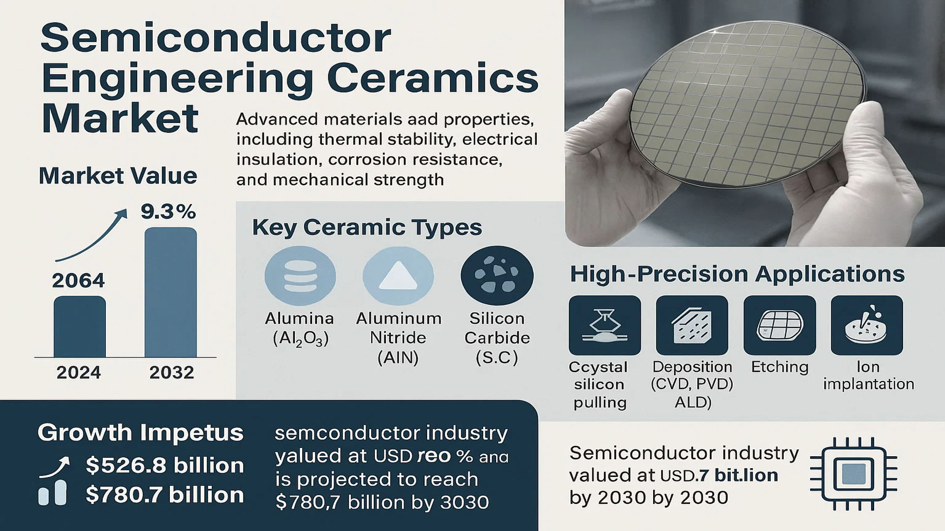
The global Semiconductor Engineering Ceramics Market was valued at 2667 million in 2024 and is projected to reach US$ 4903 million by 2032, at a CAGR of 9.3% during the forecast period.
Semiconductor Engineering Ceramics are advanced structural ceramic components engineered for use in semiconductor wafer processing and fabrication. These materials are critical due to their exceptional properties, including high thermal stability, excellent electrical insulation, corrosion resistance, and mechanical strength. Key ceramic types include Aluminas (Al2O3), Aluminum Nitride (AlN), Silicon Carbide (SiC), and Silicon Nitride (Si3N4), which are utilized in various high-precision applications such as crystal silicon pulling, deposition (CVD, PVD, ALD), etching, ion implantation, lithography, and wafer handling.
The market is experiencing robust growth driven by the expansion of the global semiconductor industry, which was valued at USD 526.8 billion in 2023 and is projected to reach USD 780.7 billion by 2030. This growth is further accelerated by the rapid expansion of semiconductor manufacturing (wafer fabrication), projected to grow from USD 251.7 billion in 2023 to USD 506.5 billion by 2030, at a CAGR of 40.49%. The market is highly concentrated, with the top nine players holding over 88% share. Japanese manufacturers dominate with approximately 68% market share, followed by US players at 10.2%, while European and South Korean firms hold 10.3% and 5.87%, respectively. Key players such as NGK Insulators, Kyocera, Coorstek, and Ferrotec are strengthening their positions through strategic expansions and acquisitions to meet the rising demand.
MARKET DYNAMICS
MARKET DRIVERS
Rapid Expansion of Semiconductor Manufacturing to Fuel Demand for Engineering Ceramics
The global semiconductor manufacturing market is projected to grow from $251.7 billion in 2023 to $506.5 billion by 2030, representing a compound annual growth rate of 40.49% during the forecast period. This explosive growth directly drives the semiconductor engineering ceramics market, as these advanced materials are essential components in wafer fabrication equipment. Engineering ceramics provide critical properties including exceptional thermal stability, chemical resistance, and electrical insulation required for semiconductor processing environments. The increasing complexity of semiconductor devices, particularly with the transition to smaller nanometer nodes and 3D architectures, necessitates more sophisticated ceramic components that can withstand extreme processing conditions while maintaining dimensional stability and purity standards.
Advancements in Semiconductor Equipment Technologies to Accelerate Market Growth
Technological innovations in semiconductor manufacturing equipment are creating substantial demand for specialized engineering ceramics. The development of extreme ultraviolet (EUV) lithography systems, which operate at wavelengths of 13.5 nanometers, requires ceramic components with ultra-high precision and stability. Similarly, advancements in atomic layer deposition (ALD) and chemical vapor deposition (CVD) systems demand ceramics that can maintain performance at temperatures exceeding 1000°C while resisting corrosive process gases. The increasing adoption of silicon carbide and gallium nitride semiconductors for power electronics applications further drives the need for specialized ceramic substrates and components that can handle higher operating temperatures and power densities compared to traditional silicon-based devices.
Growing Investment in Semiconductor Fabrication Facilities to Stimulate Market Expansion
Massive investments in new semiconductor fabrication plants worldwide are creating unprecedented demand for engineering ceramics. Recent initiatives including the CHIPS Act in the United States have committed over $52 billion in semiconductor manufacturing incentives, leading to numerous new fabrication facility announcements. Similarly, countries across Asia and Europe are implementing substantial semiconductor investment programs. Each new fabrication facility represents billions of dollars in equipment investment, with engineering ceramics comprising critical components across deposition, etch, lithography, and wafer handling systems. The simultaneous construction of multiple advanced fabrication facilities globally is creating a substantial backlog for ceramic components, with lead times for certain specialized ceramics extending beyond 12 months.
Furthermore, the increasing complexity of semiconductor manufacturing processes requires more ceramic components per wafer processing tool. Modern EUV lithography systems contain over 100 precision ceramic parts, while advanced etch and deposition systems utilize numerous ceramic chambers, heaters, and insulators. This trend toward higher ceramic content per equipment unit, combined with the expansion of manufacturing capacity globally, creates a multiplicative effect on market growth.
MARKET RESTRAINTS
High Manufacturing Complexity and Cost Constraints to Limit Market Penetration
The manufacturing of semiconductor-grade engineering ceramics involves extremely complex processes with stringent quality requirements that significantly constrain market expansion. These ceramics must achieve ultra-high purity levels exceeding 99.99% with precisely controlled microstructures and minimal defects. The production processes require specialized equipment including high-temperature sintering furnaces capable of reaching temperatures above 1800°C, precision machining centers with sub-micron accuracy, and cleanroom facilities meeting Class 10 or better standards. The capital investment for establishing manufacturing capacity can exceed $100 million for a medium-scale production facility, creating substantial barriers to entry and limiting the number of qualified suppliers worldwide.
Technical Challenges in Ceramic Material Development to Hinder Market Progress
Developing advanced ceramic materials that meet the evolving requirements of semiconductor manufacturing presents significant technical challenges. As semiconductor devices shrink to 3 nanometer nodes and below, ceramic components must achieve dimensional stability within 0.1 micrometers while maintaining mechanical strength and thermal properties. The development of new ceramic compositions that can withstand increasingly aggressive process chemistries, including fluorine-based etch gases and high-pressure processing environments, requires extensive research and development investment. Additionally, achieving the necessary surface finish requirements, often below 0.1 micrometer roughness, demands advanced polishing techniques that are both time-consuming and costly to implement at production scales.
Supply Chain Constraints and Raw Material Availability to Restrict Market Growth
The semiconductor engineering ceramics market faces substantial constraints from limited availability of high-purity raw materials and specialized manufacturing equipment. Key raw materials including high-purity alumina powder, silicon carbide precursors, and aluminum nitride compounds require sophisticated processing facilities that are concentrated among few global suppliers. Recent disruptions in the global supply chain have highlighted the vulnerability of these material supply networks, with lead times for certain ceramic precursors extending beyond six months. Additionally, the specialized equipment required for ceramic manufacturing, including hot isostatic presses and precision grinding machines, often has delivery timelines exceeding 12 months, further constraining capacity expansion efforts.
MARKET CHALLENGES
Stringent Quality and Performance Requirements to Challenge Market Participants
Semiconductor manufacturers impose exceptionally rigorous quality standards on engineering ceramics that present significant challenges for market participants. Components must demonstrate zero particulate generation during operation, maintain dimensional stability across temperature variations up to 500°C, and exhibit consistent electrical properties under varying environmental conditions. The qualification process for new ceramic components typically requires 12-18 months of testing and validation, including extensive life cycle testing and failure mode analysis. Any deviation from specification, even at parts-per-billion contamination levels, can result in component rejection and substantial financial losses for manufacturers.
Other Challenges
Technical Expertise Shortage
The specialized nature of semiconductor ceramic manufacturing has created a critical shortage of qualified technical professionals. The field requires expertise in materials science, precision engineering, and semiconductor processes, with experienced professionals commanding premium compensation packages. The aging workforce in established ceramic manufacturing regions compounds this challenge, as knowledge transfer to younger generations proves difficult due to the highly specialized nature of the work.
Rapid Technological Obsolescence
The pace of semiconductor technology advancement creates constant pressure on ceramic manufacturers to develop new materials and processes. Ceramic components developed for current generation equipment may become obsolete within 2-3 years as semiconductor manufacturers transition to new technology nodes. This rapid obsolescence cycle requires continuous research and development investment while creating uncertainty in production planning and capacity utilization.
MARKET OPPORTUNITIES
Emerging Applications in Advanced Packaging to Create New Growth Avenues
The rapid growth of advanced semiconductor packaging technologies presents significant opportunities for engineering ceramics. The market for heterogeneous integration and 3D packaging is projected to grow at over 20% annually, driven by applications in artificial intelligence, high-performance computing, and 5G communications. These packaging approaches require specialized ceramic substrates with superior thermal management properties, particularly for applications involving multiple die integration and high power densities. Ceramics such as aluminum nitride and silicon carbide offer thermal conductivity values exceeding 200 W/mK, making them ideal solutions for managing heat dissipation in advanced packaging architectures. The development of ceramic interposers and substrates with embedded passive components represents a particularly promising opportunity for market expansion.
Expansion into Compound Semiconductor Manufacturing to Offer Growth Potential
The growing adoption of compound semiconductors based on gallium nitride and silicon carbide creates substantial opportunities for engineering ceramics. The market for silicon carbide power devices is projected to exceed $10 billion by 2030, driven by applications in electric vehicles, renewable energy, and industrial power systems. Manufacturing these devices requires specialized ceramic components that can withstand the higher processing temperatures and more aggressive chemistries involved in compound semiconductor fabrication. Ceramic susceptors, wafer boats, and process tubes designed for silicon carbide epitaxy and processing represent high-value applications with significant growth potential. The development of ceramics with tailored thermal expansion coefficients matching those of compound semiconductor materials presents particularly attractive opportunities for manufacturers with advanced materials capabilities.
Geographic Market Expansion and Localization Initiatives to Provide Growth Opportunities
Government initiatives worldwide to establish domestic semiconductor manufacturing capabilities are creating substantial opportunities for ceramic suppliers. The geographic diversification of semiconductor manufacturing, driven by supply chain security concerns and national strategic priorities, is prompting the development of ceramic manufacturing capacity in regions previously dependent on imports. Countries including the United States, Germany, and India are implementing programs to develop local ceramic supply chains supporting their semiconductor industries. This geographic expansion presents opportunities for both established manufacturers to expand their global footprint and new entrants to capture emerging regional demand. The trend toward supply chain localization is particularly beneficial for ceramic manufacturers capable of establishing production facilities near major semiconductor fabrication clusters, reducing logistics costs and improving responsiveness to customer needs.
SEMICONDUCTOR ENGINEERING CERAMICS MARKET TRENDS
Advanced Node Manufacturing and Miniaturization Drive Material Innovation
The relentless push towards smaller semiconductor nodes, particularly below 5nm, is fundamentally reshaping material requirements within fabrication equipment. Engineering ceramics must now exhibit unprecedented levels of purity, thermal stability, and plasma resistance to withstand the aggressive chemistries and extreme temperatures of advanced processes like Atomic Layer Deposition (ALD) and Extreme Ultraviolet (EUV) lithography. This has catalyzed a significant shift from traditional alumina (Al2O3) towards higher-performance materials such as aluminum nitride (AlN) and yttria (Y2O3)-coated components. Yttria, for instance, offers exceptional plasma erosion resistance, which is critical for etch and deposition chambers. The market for these advanced ceramics is expanding rapidly because they are essential for maintaining yield and process control at these leading-edge nodes, with demand growing in direct correlation with the increasing capital expenditure on advanced fabrication tools, which is projected to exceed $180 billion annually by 2025.
Other Trends
Geopolitical Reshoring and Supply Chain Diversification
Geopolitical tensions and a heightened focus on supply chain security are compelling major semiconductor-producing regions to invest heavily in domestic manufacturing capabilities. Initiatives like the CHIPS Act in the United States and similar policies in the European Union and Japan are funneling over $200 billion in public and private investments into new fab construction and expansion. This creates a parallel and immediate demand for the high-purity ceramic components integral to this equipment. While Japan currently dominates ceramic component production with an estimated 68% market share, these new geopolitical imperatives are actively fostering the growth of domestic and alternative supply sources in North America and Europe. This trend is not just about building fabs but also about securing the entire materials ecosystem, leading to increased R&D and production investments in engineering ceramics outside of the traditional Asian supply base.
Sustainability and Extended Component Lifespan
As semiconductor manufacturing is an energy- and resource-intensive process, there is a growing operational and financial impetus to improve sustainability. A key focus is on extending the lifespan of consumable ceramic components within fabrication equipment. Longer-lasting components reduce machine downtime for maintenance, lower the total cost of ownership, and minimize waste. This has accelerated the development and adoption of advanced coating technologies, surface treatments, and new ceramic composites designed to resist wear, corrosion, and particle generation. Manufacturers are investing in materials that can endure more wafer processing cycles before requiring replacement. This trend towards durability is increasingly a competitive differentiator for ceramic suppliers, as fab operators seek to maximize efficiency and minimize their environmental footprint while managing rising operational costs.
COMPETITIVE LANDSCAPE
Key Industry Players
Dominant Players Leverage Technical Expertise and Strategic Expansion to Maintain Market Leadership
The global semiconductor engineering ceramics market exhibits a highly consolidated structure, dominated by a handful of established players primarily from Japan and the United States. The market’s concentration is underscored by the fact that the top nine players collectively command over 88% of the global market share as of 2024. This dominance is rooted in decades of specialized material science research, extensive intellectual property portfolios, and deep-seated relationships with leading semiconductor equipment manufacturers.
NGK Insulators and Kyocera Corporation are preeminent leaders, largely due to their comprehensive product offerings that span critical applications from wafer handling and electrostatic chucks to CVD components. Their market leadership is further solidified by their significant manufacturing footprint in Japan, which accounts for approximately 68% of the global production share. These Japanese giants benefit from a synergistic ecosystem of advanced ceramics development and proximity to major semiconductor fabrication plants in Asia.
Meanwhile, U.S.-based players like Coorstek and 3M hold a vital position, representing roughly 10.2% of the market. Their growth is propelled by robust investments in R&D for next-generation ceramics, such as high-purity aluminum nitride and silicon carbide, which are essential for extreme thermal management in advanced etch and deposition tools. These companies are actively pursuing strategic acquisitions and capacity expansions to bolster their global supply chains and cater to the rising demand from North American and European semiconductor fabs.
Furthermore, companies such as Ferrotec and Morgan Advanced Materials are strengthening their positions through technological innovations and strategic partnerships. Recent developments include the introduction of ceramics with enhanced plasma resistance for dry etch applications and new grades optimized for EUV lithography systems. Their continuous focus on material purity, structural integrity, and custom engineering solutions ensures they remain critical suppliers in an industry where component failure is not an option.
List of Key Semiconductor Engineering Ceramics Companies Profiled
- NGK Insulators, Ltd. (Japan)
- Kyocera Corporation (Japan)
- Ferrotec Corporation (Japan)
- TOTO Advanced Ceramics (Japan)
- Morgan Advanced Materials plc (UK)
- Coorstek, Inc. (U.S.)
- Niterra Co., Ltd. (Japan)
- ASUZAC Fine Ceramics (Japan)
- MiCo Ceramics Co., Ltd. (South Korea)
- 3M Company (U.S.)
- CeramTec GmbH (Germany)
- Saint-Gobain (France)
Segment Analysis:
By Type
Alumina (Al2O3) Segment Commands Significant Market Share Due to Its Excellent Thermal Stability and Cost-Effectiveness
The market is segmented based on type into:
- Alumina (Al2O3)
- Aluminum Nitride (AlN)
- Silicon Carbide (SiC)
- Silicon Nitride (Si3N4)
- Others
By Application
Semiconductor Deposition Equipment Segment Leads Owing to Critical Role in Thin Film Deposition Processes
The market is segmented based on application into:
- Semiconductor Deposition Equipment
- Semiconductor Etch Equipment
- Lithography Machines
- Ion Implant Equipment
- Heat Treatment Equipment
- CMP Equipment
- Wafer Handling
- Assembly Equipment
- Others
By Region
Asia-Pacific Dominates the Market Fueled by Robust Semiconductor Manufacturing Hub
The market is segmented based on region into:
- Asia-Pacific
- North America
- Europe
- South America
- Middle East & Africa
Regional Analysis: Semiconductor Engineering Ceramics Market
Asia-Pacific
Asia-Pacific dominates the global semiconductor engineering ceramics market, holding the largest market share estimated at over 68% in 2024, driven primarily by Japan’s manufacturing prowess and substantial investments across the region. Japan is the undisputed leader, home to industry giants like NGK Insulators, Kyocera, and TOTO Advanced Ceramics, which collectively command a significant portion of global production. This regional supremacy is fueled by massive semiconductor fabrication expansion, particularly in Taiwan, South Korea, and China, where new fab constructions and technological upgrades necessitate advanced ceramic components for processes like etching, deposition, and wafer handling. The projected growth of the Asia-Pacific semiconductor manufacturing market, expected to reach over $300 billion by 2030, creates sustained demand for high-purity alumina, aluminum nitride, and silicon carbide components. While cost-competitive manufacturing prevails, there is a strong emphasis on innovation to meet the stringent purity and thermal management requirements of next-generation nodes below 5nm.
North America
North America represents a technologically advanced and innovation-driven market for semiconductor engineering ceramics, accounting for approximately 10.2% of the global share. The region is characterized by strong presence of key players like Coorstek and 3M, alongside significant R&D activities focused on developing ceramics for extreme applications in EUV lithography and advanced packaging. Government initiatives, including the CHIPS and Science Act, which allocates over $52 billion for domestic semiconductor research and manufacturing, are catalyzing investments in new fabrication facilities. This, in turn, drives demand for high-performance ceramic components that offer exceptional thermal stability, corrosion resistance, and minimal particulate contamination. The focus is squarely on materials that enable next-generation chip manufacturing, with a strong collaborative ecosystem between national labs, universities, and ceramic manufacturers pushing the boundaries of material science.
Europe
Europe holds a stable and significant position in the semiconductor engineering ceramics market, with a share of about 10.3%. The region benefits from a strong industrial base and the presence of leading technical ceramic companies such as Morgan Advanced Materials and CeramTec. The European market is driven by stringent quality standards and a focus on high-value, precision components for semiconductor equipment used in research institutions and specialized manufacturing sites. The EU’s Chips Act, aiming to double its global market share in semiconductors to 20% by 2030, is expected to stimulate local demand for engineering ceramics. However, the market growth is tempered by higher production costs compared to Asia and a more fragmented manufacturing landscape. Innovation is focused on sustainability and developing ceramics with enhanced lifecycle performance for applications in ion implant and heat treatment equipment.
South America
The semiconductor engineering ceramics market in South America is nascent and represents a minor fraction of the global landscape. The region currently lacks large-scale semiconductor fabrication infrastructure, resulting in limited direct demand for these specialized components. Any existing demand is primarily met through imports for maintenance and servicing of semiconductor assembly and test equipment. Economic volatility and a focus on commodity exports rather than high-tech manufacturing have historically hindered the development of a local advanced ceramics supply chain. While countries like Brazil have some electronic manufacturing, the scale is insufficient to drive significant market growth for engineering ceramics in the foreseeable future. Opportunities exist mainly for multinational suppliers serving multinational corporations with regional operations.
Middle East & Africa
The Middle East & Africa region is an emerging and very small player in the global semiconductor engineering ceramics market. The market is primarily import-dependent, with demand stemming from a handful of research facilities and small-scale electronics assembly plants. Countries like Israel show some technological advancement in specific niches, but the region lacks the foundational semiconductor fabrication ecosystem required to generate substantial demand for engineering ceramics. Long-term growth potential is tied to broader economic diversification plans in nations like Saudi Arabia and the UAE, which include investments in technology and manufacturing. However, progress is expected to be slow, constrained by a lack of local expertise, high setup costs, and intense global competition from established manufacturing hubs.
Report Scope
This market research report provides a comprehensive analysis of the global and regional Semiconductor Engineering Ceramics markets, covering the forecast period 2025–2032. It offers detailed insights into market dynamics, technological advancements, competitive landscape, and key trends shaping the industry.
Key focus areas of the report include:
- Market Size & Forecast: Historical data and future projections for revenue, unit shipments, and market value across major regions and segments.
- Segmentation Analysis: Detailed breakdown by product type, technology, application, and end-user industry to identify high-growth segments and investment opportunities.
- Regional Outlook: Insights into market performance across North America, Europe, Asia-Pacific, Latin America, and the Middle East & Africa, including country-level analysis where relevant.
- Competitive Landscape: Profiles of leading market participants, including their product offerings, R&D focus, manufacturing capacity, pricing strategies, and recent developments such as mergers, acquisitions, and partnerships.
- Technology Trends & Innovation: Assessment of emerging technologies, integration of AI/IoT, semiconductor design trends, fabrication techniques, and evolving industry standards.
- Market Drivers & Restraints: Evaluation of factors driving market growth along with challenges, supply chain constraints, regulatory issues, and market-entry barriers.
- Stakeholder Analysis: Insights for component suppliers, OEMs, system integrators, investors, and policymakers regarding the evolving ecosystem and strategic opportunities.
Primary and secondary research methods are employed, including interviews with industry experts, data from verified sources, and real-time market intelligence to ensure the accuracy and reliability of the insights presented.
FREQUENTLY ASKED QUESTIONS:
What is the current market size of Global Semiconductor Engineering Ceramics Market?
-> Semiconductor Engineering Ceramics Market was valued at 2667 million in 2024 and is projected to reach US$ 4903 million by 2032, at a CAGR of 9.3% during the forecast period.
Which key companies operate in Global Semiconductor Engineering Ceramics Market?
-> Key players include NGK Insulators, Kyocera, Ferrotec, TOTO Advanced Ceramics, Coorstek, Morgan Advanced Materials, Niterra Co., Ltd., ASUZAC Fine Ceramics, and 3M, among others. The top nine players collectively hold a market share exceeding 88%.
What are the key growth drivers?
-> Key growth drivers include the expansion of global semiconductor manufacturing capacity, which is projected to grow from USD 251.7 billion in 2023 to USD 506.5 billion by 2030, and the critical role of advanced ceramics in semiconductor fabrication equipment for processes like deposition, etching, and wafer handling.
Which region dominates the market?
-> Asia-Pacific is the dominant region, driven by major semiconductor manufacturing hubs. Japan is the leading country, with manufacturers holding approximately 68% of the global market share.
What are the emerging trends?
-> Emerging trends include the development of ultra-high purity ceramic materials for next-generation nodes below 3nm, integration of ceramics in EUV lithography systems, and advanced manufacturing techniques to meet the extreme thermal and chemical resistance requirements of new fabrication processes.

Get Sample Report PDF for Exclusive Insights
Report Sample Includes
- Table of Contents
- List of Tables & Figures
- Charts, Research Methodology, and more...