MARKET INSIGHTS
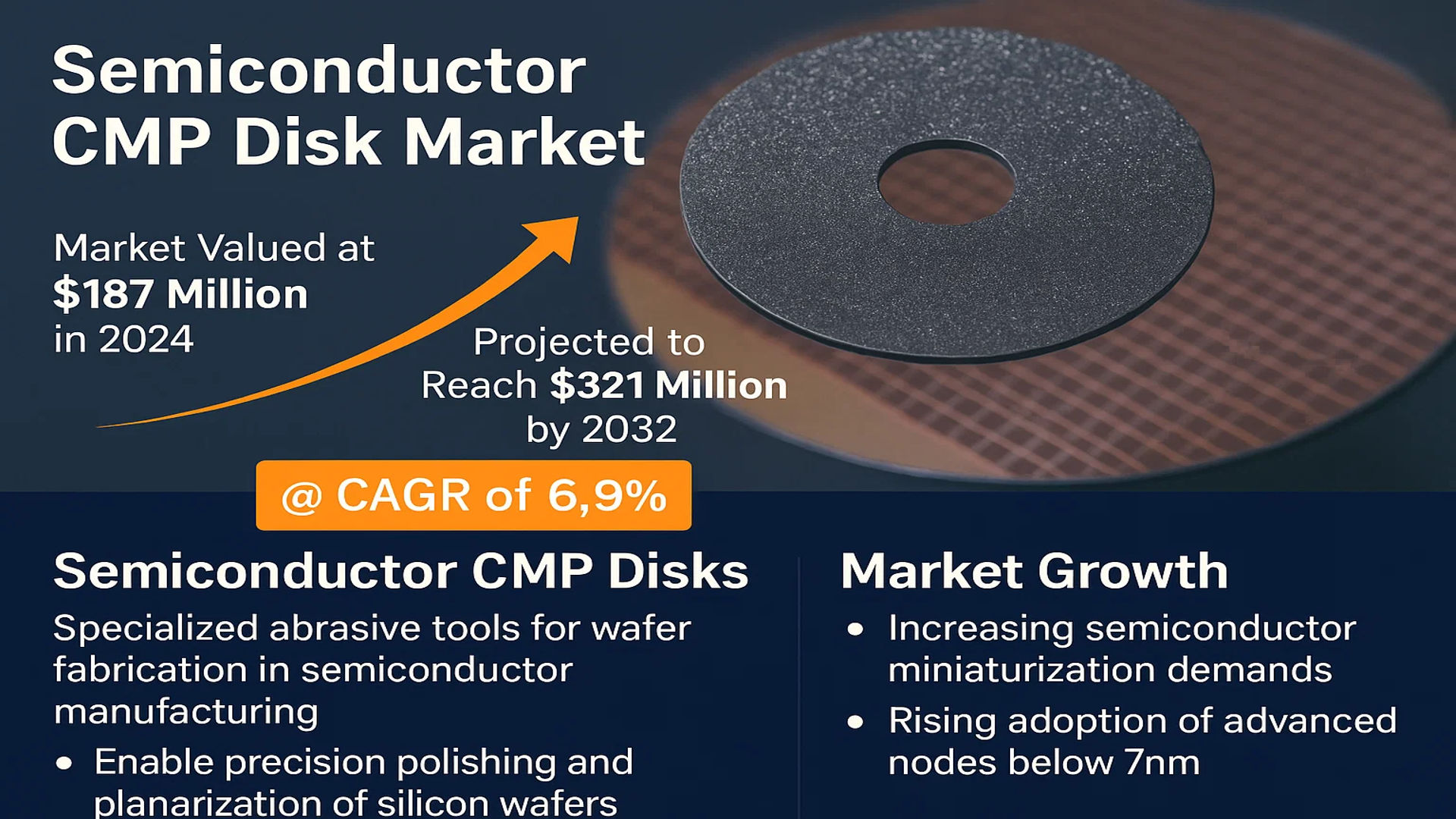
The global Semiconductor CMP Disk Market was valued at 187 million in 2024 and is projected to reach US$ 321 million by 2032, at a CAGR of 6.9% during the forecast period.
Semiconductor CMP (Chemical Mechanical Planarization) Disks are specialized abrasive tools critical for wafer fabrication in semiconductor manufacturing. These disks enable precision polishing and planarization of silicon wafers during integrated circuit (IC) production, ensuring nanometer-level surface uniformity for subsequent lithography and deposition processes. The technology primarily utilizes diamond-embedded or composite abrasive materials to achieve the required material removal rates while maintaining surface integrity.
The market growth is driven by increasing semiconductor miniaturization demands and rising adoption of advanced nodes below 7nm, where CMP becomes even more crucial. While wafer size transitions toward 300mm dominate current demand, emerging applications in advanced packaging and MEMS devices present new opportunities. Key manufacturers like Kinik Company and 3M are innovating with advanced diamond matrix formulations to address the growing need for defect-free polishing in next-generation semiconductor fabrication.
MARKET DYNAMICS
MARKET DRIVERS
Growing Demand for Advanced Semiconductor Nodes to Accelerate CMP Disk Adoption
The semiconductor industry’s relentless push toward smaller process nodes below 7nm is driving unprecedented demand for precision planarization solutions. As chipmakers transition to 5nm and 3nm processes, the tolerance for surface irregularities has reduced to atomic-scale levels. This has elevated the importance of CMP disks in achieving the required surface uniformity, with the market for advanced node fabrication tools growing at nearly twice the rate of mature nodes. The global foundry capacity for nodes below 10nm is projected to increase by over 60% between 2024 and 2027, creating substantial demand for high-performance CMP consumables.
Expansion of 300mm Wafer Production to Fuel Market Growth
The semiconductor industry continues its transition toward 300mm wafer manufacturing, with this segment accounting for approximately 78% of global wafer area capacity in 2024. This shift is particularly significant for CMP disk manufacturers as larger wafers require more rigorous planarization to maintain yield rates. The ongoing construction of new 300mm fabs across Asia and North America, with over 30 major facilities projected to come online by 2026, is creating strong demand-supply dynamics for CMP consumables. Investments in wafer fabrication equipment are exceeding $100 billion annually, a significant portion of which is allocated to CMP and related material solutions.
Increasing Complexity of 3D NAND and DRAM Architectures to Drive Innovation
The memory sector’s transition to vertically-stacked architectures presents both challenges and opportunities for CMP technology. As 3D NAND layers surpass 200 and DRAM scales below 15nm, the planarization requirements have become more demanding. This has led to development of specialized CMP disk formulations capable of handling complex material stacks with precise removal rates. Memory manufacturers are increasingly partnering with CMP disk suppliers to co-develop application-specific solutions, creating new revenue streams in what has traditionally been a commodity market segment.
MARKET RESTRAINTS
High Production Costs and Margin Pressures to Limit Market Expansion
The semiconductor CMP disk market faces significant cost challenges, with raw material expenses accounting for approximately 45-50% of total production costs. The specialized diamond and composite materials required for high-performance disks have seen price increases of 18-22% since 2022 due to supply chain disruptions. While wafer fabs negotiate bulk purchase discounts exceeding 30%, CMP disk manufacturers struggle to pass through these cost increases, leading to compressed margins that average 15-18% industry-wide. This financial pressure limits R&D investment capacity at a time when technological demands are accelerating.
Technical Challenges in Next-Generation Material Integration
The introduction of novel semiconductor materials like cobalt interconnects and high-mobility channel materials presents significant technical hurdles for CMP processes. These materials often demonstrate unpredictable removal characteristics and require specialized disk formulations with tightly controlled abrasion profiles. The development cycles for compatible CMP solutions now average 18-24 months, creating bottlenecks in advanced node transitions. Furthermore, the industry’s shift toward heterogeneous integration using chiplets introduces additional planarization challenges that existing disk technologies struggle to address comprehensively.
Regulatory and Environmental Constraints on Material Usage
Increasing environmental regulations are impacting the composition and manufacturing of CMP disks globally. Restrictions on certain abrasive materials and binding agents have forced multiple reformulations across the industry, with compliance costs adding 5-7% to production expenses. The classification of certain CMP byproducts as hazardous waste in multiple jurisdictions has also increased disposal costs and liability exposure. These regulatory pressures are particularly challenging for small and medium-sized suppliers that lack the resources to maintain multiple product formulations for different regional markets.
MARKET OPPORTUNITIES
Emerging Materials Science Innovations to Create New Market Segments
Breakthroughs in advanced materials are creating opportunities for next-generation CMP disk solutions. The development of nanostructured diamond composites and engineered abrasives offers potential for disks with up to 40% longer service life and more consistent performance characteristics. Several leading suppliers have already introduced disks incorporating these materials, achieving 15-20% improvements in planarization uniformity. These innovations are particularly valuable for memory applications where consistent performance across wafer batches directly correlates with yield improvements of 2-3 percentage points.
Expansion of China’s Domestic Semiconductor Ecosystem
China’s aggressive investments in semiconductor self-sufficiency are creating a parallel market for CMP disk manufacturers. The country’s domestic wafer fab capacity is projected to grow at a CAGR of 12% through 2030, outpacing global growth rates by nearly 4 percentage points. While international players currently dominate the high-end segment, local suppliers are capturing increasing share in mature nodes, supported by government procurement policies. This bifurcation of the market presents opportunities for technology licensing and joint ventures, with several global firms already establishing local production partnerships.
Integration of AI and Advanced Process Control Solutions
The incorporation of machine learning into CMP process control is opening new frontiers for disk performance optimization. Real-time monitoring systems can now predict disk wear patterns with 90%+ accuracy, enabling preventive maintenance that reduces unplanned tool downtime by 30-35%. Several major foundries have begun specifying smart disk solutions that integrate with these systems, creating a premium product segment with margins 8-10 points above conventional offerings. The market for intelligent CMP consumables is expected to grow at 25% annually through 2030 as these technologies become standard in high-volume production environments.
MARKET CHALLENGES
Intensifying Supply Chain Vulnerabilities in Critical Materials
The CMP disk industry faces growing supply chain risks for key raw materials, particularly synthetic diamonds and specialty binders. Over 70% of synthetic diamond production is concentrated in a limited number of facilities, creating single points of failure in the supply network. The 2023 disruption in diamond feedstock availability caused delivery delays of up to six months for some CMP disk models, forcing fabs to extend disk usage beyond recommended cycles. Such incidents highlight the need for diversification, but establishing alternative supply chains requires capital investments that many mid-tier suppliers cannot readily absorb.
Technological Disruption from Alternative Planarization Methods
Emerging deposition and etching techniques threaten to displace certain CMP applications, particularly in back-end-of-line processes. Atomic layer deposition and selective area removal technologies are achieving dimensional control comparable to CMP for some applications, without the consumable costs. While these methods currently address only about 15% of traditional CMP use cases, their adoption is growing at 35% annually in advanced packaging applications. CMP disk manufacturers must accelerate innovation cycles to maintain value propositions as these alternatives mature.
Workforce Shortages in Precision Manufacturing
The specialized nature of CMP disk production creates significant workforce challenges, with the industry facing a 20-25% shortage of qualified technicians and engineers. The skills required for disk formulation and quality control typically require 3-5 years of hands-on experience, creating a bottleneck in production scaling. This talent gap is particularly acute in regions with competing high-tech industries, where semiconductor material specialists are being drawn to higher-paying sectors. The resulting wage inflation has added 7-9% to production costs since 2020, with no immediate resolution in sight as educational pipelines struggle to keep pace with industry needs.
SEMICONDUCTOR CMP DISK MARKET TRENDS
Rising Demand for Advanced Semiconductor Devices Driving CMP Disk Adoption
The semiconductor industry is witnessing rapid advancements in device miniaturization and performance optimization, fueling the demand for Chemical Mechanical Planarization (CMP) disks. As modern chips increasingly rely on complex multi-layer architectures, manufacturers require ultra-precise surface finishing solutions to maintain yield rates. The global market is projected to grow at 6.9% CAGR through 2032, reaching $321 million, as foundries expand production capacity to meet demand for 7nm and below process nodes. While traditional silicon wafers continue to dominate, emerging materials like silicon carbide and gallium nitride are creating new application areas for specialized CMP solutions.
Other Trends
Transition Toward Larger Wafer Sizes
The industry’s shift toward 300mm wafers is reshaping CMP disk requirements, as larger substrates demand more uniform planarization across expanded surface areas. This transition has prompted suppliers to develop next-generation diamond-embedded disks with improved wear resistance and consistency. Currently, 300mm wafer production accounts for over 60% of CMP disk consumption, though 200mm applications remain vital for legacy chips and specialty devices. The bifurcation between advanced-node and mature-node manufacturing is creating parallel opportunities across the CMP disk value chain.
Material Innovations and Process Optimization
Manufacturers are introducing novel composite materials and grain structures to address challenges in emerging semiconductor applications. The diamond CMP disk segment, representing over 70% of the market by value, continues to evolve through advanced bond formulations and controlled abrasive distributions. Concurrently, process optimization efforts are reducing consumable waste while improving mean time between replacements (MTBR). This dual focus on material science and operational efficiency helps chipmakers balance precision requirements with cost considerations across high-volume production lines.
COMPETITIVE LANDSCAPE
Key Industry Players
Leadership in Semiconductor CMP Disk Market Driven by Technical Expertise and Material Innovation
The global Semiconductor CMP Disk market demonstrates a competitive yet moderately fragmented structure, with established players competing alongside regional specialists. Kinik Company emerges as a dominant force, leveraging Taiwan-based manufacturing excellence and strategic partnerships with semiconductor foundries. The company’s proprietary diamond abrasive technology gives it an edge in planarization efficiency, capturing an estimated 18-22% global revenue share in 2024. This leadership stems from continuous R&D, with Kinik allocating over 7% of annual revenues toward developing next-generation CMP solutions.
3M’s Advanced Materials Division has made significant inroads through its diversified chemical-mechanical polishing portfolio. The company’s recent introduction of nanocomposite CMP disks has gained traction among leading logic chip manufacturers, particularly for sub-7nm node applications. Meanwhile, EHWA DIAMOND from South Korea continues to expand its market presence, capitalizing on growing domestic semiconductor production and Asian supply chain advantages. Their specialization in tungsten and copper polishing applications positions them strongly in memory chip manufacturing segments.
The competitive environment intensifies as companies pursue technological differentiation through material science breakthroughs. Asahi Diamond recently unveiled its low-defect CMP disk series, reducing wafer scratch rates by approximately 30% compared to industry benchmarks. Such innovations are critical as semiconductor nodes advance, where surface imperfections can significantly impact yield rates. Meanwhile, Chinese manufacturers like NanJing Sanchao Advanced Materials are gaining market share through cost-competitive solutions tailored for mature process nodes, particularly in the 200mm wafer segment.
List of Key Semiconductor CMP Disk Manufacturers
- Kinik Company (Taiwan)
- 3M Company (U.S.)
- Saesol Diamond (South Korea)
- EHWA DIAMOND (South Korea)
- Asahi Diamond Industrial (Japan)
- NanJing Sanchao Advanced Materials (China)
- Hubei Dinglong (China)
- Fujimi Incorporated (Japan)
- DuPont de Nemours, Inc. (U.S.)
Segment Analysis:
By Type
Diamond CMP Disk Segment Leads Due to Superior Performance and Longer Lifespan
The market is segmented based on type into:
- Diamond CMP Disk
- Subtypes: Resin-bonded, Metal-bonded, and others
- Silicon Carbide CMP Disk
- Ceramic CMP Disk
- Subtypes: Alumina-based, Zirconia-based, and others
- Others
By Application
300mm Wafer Segment Dominates Due to High Demand in Advanced Semiconductor Manufacturing
The market is segmented based on application into:
- 300mm Wafer
- 200mm Wafer
- Others
By Material Type
Copper Segment Leads Due to Widespread Use in Interconnect Applications
The market is segmented based on material type into:
- Copper
- Tungsten
- Silicon Nitride
- Silicon Oxide
- Silicon
- Others
By End-User
Foundries Segment Dominates Due to High Volume Semiconductor Production
The market is segmented based on end-user into:
- Foundries
- Integrated Device Manufacturers (IDMs)
- Memory Manufacturers
- Others
Regional Analysis: Semiconductor CMP Disk Market
Asia-Pacific
Asia-Pacific dominates the global Semiconductor CMP Disk market, accounting for the highest revenue share in 2024, with China leading due to its rapidly expanding semiconductor manufacturing industry. The region benefits from strong government support, such as China’s $150 billion semiconductor investment plan, and the presence of major foundries like TSMC in Taiwan and Samsung in South Korea. Japan remains a key player in advanced CMP disk technology, while countries like India are emerging as growth markets with new semiconductor fabrication plants under development. Increasing demand for 300mm wafers, particularly for applications in AI and 5G chips, is driving innovation in precision CMP disk solutions across the region.
North America
North America maintains technological leadership in semiconductor manufacturing processes, with the U.S. hosting critical R&D centers for CMP disk development. The region shows strong adoption of diamond-based CMP disks for advanced node wafer processing (5nm and below). Major semiconductor companies like Intel and GlobalFoundries are investing in domestic production capacity, supported by the CHIPS Act funding of $52 billion, which indirectly stimulates demand for high-performance CMP consumables. However, the shift of volume manufacturing to Asia has led to a focus on specialty and low-volume high-mix production in North America, affecting the product mix of CMP disks used in the region.
Europe
Europe’s Semiconductor CMP Disk market is characterized by specialization in advanced research and niche applications, particularly for MEMS and power semiconductors. Countries like Germany and France host leading equipment manufacturers that drive demand for high-precision CMP solutions. The European Chips Act, with €43 billion in planned investments, aims to strengthen semiconductor sovereignty and is expected to boost CMP disk demand. However, the region faces challenges from limited large-scale wafer fabrication compared to Asia, causing slower adoption rates for high-volume CMP disk solutions. Sustainability initiatives are pushing manufacturers toward longer-lasting and reusable disk technologies.
Middle East & Africa
The MEA region represents an emerging market for Semiconductor CMP Disks, with initial growth centered around Israel’s established semiconductor design industry and the UAE’s technology diversification efforts. While wafer fabrication capacity remains limited, increasing investments in technology parks and research facilities are creating early-stage demand. The market faces infrastructure challenges in supporting advanced semiconductor manufacturing but shows potential as global players consider geographical diversification of their supply chains. Partnerships with European and Asian technology providers are helping build the region’s capabilities in semiconductor materials processing.
South America
South America’s Semiconductor CMP Disk market remains in nascent stages, with Brazil showing the most activity through its modest but growing semiconductor packaging and testing operations. The lack of major wafer fabrication facilities limits immediate market potential, though increasing electronics manufacturing in the region supports steady demand for maintenance and small-scale production requirements. Economic volatility and limited local expertise in advanced semiconductor materials create barriers to rapid market expansion but present opportunities for technology transfer and partnerships with established global suppliers.
Report Scope
This market research report provides a comprehensive analysis of the global Semiconductor CMP Disk market, covering the forecast period 2024–2032. It offers detailed insights into market dynamics, technological advancements, competitive landscape, and key trends shaping the industry.
Key focus areas of the report include:
- Market Size & Forecast: Historical data and future projections for revenue, unit shipments, and market value across major regions and segments. The global Semiconductor CMP Disk market was valued at USD 187 million in 2024 and is projected to reach USD 321 million by 2032, growing at a CAGR of 6.9%.
- Segmentation Analysis: Detailed breakdown by product type (Diamond CMP Disk, Others) and application (300mm Wafer, 200mm Wafer, Others) to identify high-growth segments and investment opportunities.
- Regional Outlook: Insights into market performance across North America, Europe, Asia-Pacific, Latin America, and the Middle East & Africa. The U.S. and China are key markets, with Asia-Pacific showing the highest growth potential.
- Competitive Landscape: Profiles of leading market participants, including Kinik Company, 3M, Saesol Diamond, EHWA DIAMOND, Asahi Diamond, NanJing Sanchao Advanced Materials, and Hubei Dinglong, covering their product offerings, R&D focus, and recent developments.
- Technology Trends & Innovation: Assessment of emerging CMP disk technologies, integration of advanced materials, and evolving semiconductor fabrication techniques.
- Market Drivers & Restraints: Evaluation of factors driving market growth such as semiconductor industry expansion, along with challenges including supply chain constraints and material costs.
- Stakeholder Analysis: Insights for semiconductor manufacturers, equipment suppliers, investors, and policymakers regarding the evolving CMP disk ecosystem and strategic opportunities.
Primary and secondary research methods are employed, including interviews with industry experts, data from verified sources, and real-time market intelligence to ensure the accuracy and reliability of the insights presented.
FREQUENTLY ASKED QUESTIONS:
What is the current market size of Global Semiconductor CMP Disk Market?
-> Semiconductor CMP Disk Market was valued at 187 million in 2024 and is projected to reach US$ 321 million by 2032, at a CAGR of 6.9% during the forecast period.
Which key companies operate in Global Semiconductor CMP Disk Market?
-> Key players include Kinik Company, 3M, Saesol Diamond, EHWA DIAMOND, Asahi Diamond, NanJing Sanchao Advanced Materials, and Hubei Dinglong.
What are the key growth drivers?
-> Key growth drivers include increasing semiconductor production, demand for advanced ICs, and technological advancements in wafer fabrication.
Which region dominates the market?
-> Asia-Pacific is the largest and fastest-growing market, driven by semiconductor manufacturing hubs in China, Taiwan, South Korea, and Japan.
What are the emerging trends?
-> Emerging trends include development of ultra-precise diamond disks, eco-friendly CMP solutions, and integration with Industry 4.0 manufacturing systems.

Get Sample Report PDF for Exclusive Insights
Report Sample Includes
- Table of Contents
- List of Tables & Figures
- Charts, Research Methodology, and more...


