MARKET INSIGHTS
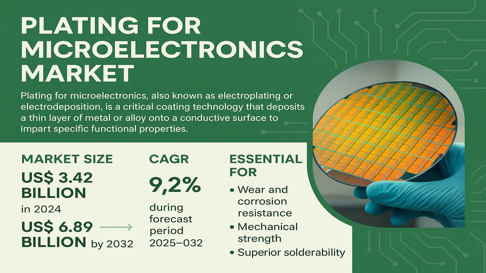
The global Plating for Microelectronics Market size was valued at US$ 3.42 billion in 2024 and is projected to reach US$ 6.89 billion by 2032, at a CAGR of 9.2% during the forecast period 2025-2032.
Plating for microelectronics, also known as electroplating or electrodeposition, is a critical coating technology that deposits a thin layer of metal or alloy onto a conductive surface to impart specific functional properties. This process is fundamental in the fabrication of microelectronic components, where the object to be plated acts as the cathode and the plating material as the anode. Immersed in an electrolyte solution and subjected to an electrical current, an oxidation/reduction reaction deposits metallic ions onto the cathode surface.
This technology is essential for enhancing wear and corrosion resistance, improving mechanical strength, and ensuring superior solderability in components. Precious metal coatings, such as gold, are particularly vital for the electronics and semiconductor industries because they provide excellent electrical conductivity and reliability. The market’s robust growth is primarily driven by the relentless miniaturization of electronic devices, the expansion of 5G infrastructure, and the rising production of advanced printed circuit boards (PCBs) and integrated circuits (ICs). Key players, including Heraeus, Atotech, and Mitsubishi Materials Corporation, are continuously innovating to develop more efficient and environmentally sustainable plating chemistries to meet evolving industry demands.
MARKET DYNAMICS
MARKET DRIVERS
Proliferation of Advanced Electronics and Miniaturization Trends to Accelerate Market Expansion
The global plating for microelectronics market is experiencing robust growth driven by the relentless advancement in electronic device miniaturization and the increasing complexity of integrated circuits. As semiconductor nodes shrink below 7nm and 5nm, the demand for precision plating solutions that ensure reliable electrical connectivity, corrosion resistance, and thermal management has surged. The market for advanced packaging, which heavily relies on plating technologies, is projected to grow at a compound annual growth rate of over 8% through 2030, underscoring the critical role of plating in next-generation electronics. Furthermore, the expansion of 5G infrastructure, IoT devices, and automotive electronics necessitates high-performance plating for components such as connectors, substrates, and interposers, creating sustained demand across multiple high-growth sectors.
Rising Adoption of Renewable Energy and Electric Vehicles to Fuel Demand
The global shift toward renewable energy and electric mobility is significantly boosting the plating for microelectronics market. Solar energy systems, wind turbines, and energy storage solutions require sophisticated power electronics and control systems where plating ensures durability and efficient electrical performance. Similarly, electric vehicles utilize extensive electronic systems for battery management, power conversion, and autonomous driving features, all dependent on high-reliability plating. The electric vehicle market is anticipated to grow at a compound annual growth rate of approximately 29% over the next five years, directly correlating with increased consumption of plating chemicals and processes. This trend is complemented by government initiatives worldwide promoting clean energy and sustainable transportation, further accelerating the need for advanced microelectronic plating solutions.
Moreover, the ongoing innovation in plating chemistries, such as the development of environmentally friendly alternatives and processes with superior throwing power, enables manufacturers to meet stringent performance and regulatory requirements. These advancements not only enhance product lifespan but also reduce failure rates in critical applications, reinforcing market growth.
➤ For instance, major automotive manufacturers are increasingly partnering with plating solution providers to develop custom formulations for high-temperature and high-voltage applications, ensuring reliability under extreme operating conditions.
Furthermore, the expansion of semiconductor fabrication facilities, particularly in Asia and North America, coupled with increased investments in R&D by key industry players, is expected to drive substantial growth throughout the forecast period.
MARKET CHALLENGES
Environmental Regulations and Waste Management Complexities to Impede Market Progress
The plating for microelectronics industry faces significant challenges due to increasingly stringent environmental regulations governing the use and disposal of hazardous chemicals. Traditional plating processes often involve toxic substances such as cyanides, heavy metals, and volatile organic compounds, which are subject to strict controls under various international and regional frameworks. Compliance with these regulations requires substantial investment in waste treatment systems, process modifications, and monitoring, increasing operational costs for manufacturers. In regions with rigorous environmental policies, permitting delays and the need for continuous compliance reporting can slow down production scaling and innovation.
Other Challenges
Supply Chain Vulnerabilities
The reliance on critical raw materials, including precious metals like gold and silver, exposes the market to price volatility and supply disruptions. Geopolitical tensions, trade restrictions, and mining output fluctuations can lead to unpredictable cost increases and material shortages, affecting production timelines and profit margins.
Technical Process Limitations
Achieving uniform plating thickness on highly complex and miniaturized components remains a persistent technical challenge. Variations in substrate geometry, current density distribution, and bath chemistry can result in defects such as voids, nodules, or insufficient coverage, leading to yield losses and reliability issues in final products.
MARKET RESTRAINTS
High Capital and Operational Costs to Limit Market Penetration
The plating for microelectronics market is constrained by the substantial capital investment required for establishing and maintaining advanced plating facilities. State-of-the-art electroplating and electrodes plating equipment, along with associated automation and quality control systems, represent significant upfront costs. Additionally, ongoing expenses related to chemical replenishment, waste treatment, energy consumption, and compliance management further elevate the total cost of ownership. These financial barriers are particularly challenging for small and medium-sized enterprises seeking to enter or expand within the market, limiting broader adoption and innovation.
Moreover, the need for highly specialized personnel to operate complex plating processes and troubleshoot technical issues adds to operational expenditures. The scarcity of skilled technicians and engineers proficient in both chemistry and electronics manufacturing exacerbates this challenge, potentially leading to production inefficiencies and increased downtime.
MARKET OPPORTUNITIES
Emergence of Advanced Plating Technologies and Sustainable Solutions to Unlock New Growth Avenues
The development of innovative plating technologies, such as selective plating, pulse plating, and nanocomposite coatings, presents significant opportunities for market expansion. These advanced processes offer enhanced performance characteristics, including improved wear resistance, higher conductivity, and better compatibility with delicate substrates, meeting the evolving needs of next-generation microelectronics. The adoption of these technologies is particularly relevant in emerging applications like flexible electronics, wearable devices, and biomedical implants, where conventional plating methods may fall short.
Additionally, growing emphasis on sustainability and circular economy principles is driving research into greener plating alternatives, such as non-cyanide baths, reduced water consumption processes, and recycling of precious metals from plating waste. Companies that pioneer eco-friendly solutions are likely to gain competitive advantage and access new market segments aligned with global sustainability goals.
Strategic collaborations between material suppliers, equipment manufacturers, and end-users are accelerating innovation and commercialization of cutting-edge plating solutions. These partnerships facilitate knowledge exchange, reduce time-to-market for new technologies, and address complex application challenges, thereby creating lucrative opportunities for industry stakeholders.
PLATING FOR MICROELECTRONICS MARKET TRENDS
Miniaturization and Advanced Packaging Technologies Drive Market Evolution
The relentless push towards device miniaturization represents the most significant trend shaping the plating for microelectronics market. As semiconductor nodes shrink below 5 nanometers and advanced packaging architectures like 2.5D and 3D integration become mainstream, conventional plating techniques face substantial challenges. This has catalyzed the development of sophisticated plating chemistries capable of achieving uniform, void-free deposits in high-aspect-ratio through-silicon vias (TSVs) and ultra-fine line interconnects. The transition to fan-out wafer-level packaging (FOWLP) alone has driven a 35% increase in demand for specialized copper and tin-silver plating solutions over the past three years. Furthermore, the emergence of heterogeneous integration, where multiple die types are combined in single packages, necessitates plating processes that can accommodate diverse material systems and thermal expansion coefficients without compromising reliability or electrical performance.
Other Trends
Sustainability and Environmental Compliance
Environmental regulations and sustainability initiatives are fundamentally transforming plating chemistry formulations and process methodologies across the microelectronics sector. The industry is experiencing a pronounced shift away from traditional cyanide-based gold plating baths and hexavalent chromium processes toward more environmentally benign alternatives. This transition is particularly evident in the European and North American markets, where regulatory frameworks like REACH and RoHS have accelerated adoption of compliant chemistries. Recent developments include the commercial introduction of cyanide-free gold plating systems that maintain deposition rates exceeding 0.5 microns per minute while reducing chemical oxygen demand by over 60% compared to conventional systems. Additionally, water recycling and recovery systems are being integrated into plating lines, with leading manufacturers achieving up to 90% water reuse in closed-loop configurations, significantly reducing both environmental impact and operational costs.
Adoption of Precious Metal Alternatives and Alloy Systems
Rising precious metal costs and supply chain volatility are driving intensive research into alternative plating materials that can match the performance characteristics of gold and palladium while reducing dependency on these critical materials. The market has witnessed growing adoption of engineered alloy systems, particularly in connector and lead-frame applications where cost pressures are most acute. Nickel-palladium-gold (NiPdAu) finishes have gained substantial market share, offering comparable wire-bonding performance and corrosion resistance while reducing gold content by approximately 80% compared to traditional thick gold deposits. Simultaneously, silver-based alternatives are emerging for high-frequency applications, with new silver-tin and silver-cobalt alloys demonstrating excellent electrical conductivity and migration resistance. These material innovations are particularly crucial for automotive and 5G applications, where reliability requirements remain exceptionally stringent while cost targets become increasingly aggressive.
COMPETITIVE LANDSCAPE
Key Industry Players
Companies Strive to Strengthen their Product Portfolio to Sustain Competition
The global plating for microelectronics market exhibits a semi-consolidated competitive landscape, characterized by a dynamic mix of multinational corporations, specialized chemical suppliers, and regional leaders. This structure is driven by the critical need for high-purity, advanced plating chemistries that meet the exacting standards of semiconductor fabrication, PCB manufacturing, and MEMS production. Atotech, a subsidiary of Mitsubishi Materials Corporation, is widely recognized as a dominant force, leveraging its extensive portfolio of electroplating and electroless plating solutions for copper, nickel, gold, and tin-silver alloys. Its leadership is further solidified by a robust global service and technical support network, which is essential for high-volume electronics manufacturing clients.
JCU International and Heraeus also command significant market share, particularly in the precious metal plating segment essential for creating reliable electrical contacts and bond pads. The prominence of these players is largely attributed to their deep expertise in gold and silver plating technologies, which are indispensable for advanced packaging and high-frequency applications. Furthermore, their continuous investment in developing environmentally compliant processes, such as cyanide-free gold plating, aligns with the industry’s increasing sustainability mandates.
Additionally, strategic growth initiatives are a primary focus. Companies are actively engaging in geographical expansions, especially within the Asia-Pacific region, which accounts for over 65% of global electronics production. For instance, several key players have recently announced new production facilities or technical centers in China, South Korea, and Taiwan to be closer to major semiconductor fabs and PCB manufacturers. New product launches focusing on next-generation applications, such as plating for through-silicon vias (TSVs) in 3D integrated circuits and fine-line patterning on substrates, are expected to be major growth drivers throughout the forecast period.
Meanwhile, other established players like DOW and Moses Lake Industries are strengthening their positions through significant R&D investments aimed at creating novel plating chemistries for smaller technology nodes below 5nm. Strategic partnerships with semiconductor equipment manufacturers are also becoming more common, ensuring that plating processes are seamlessly integrated into overall fabrication workflows. This collaborative approach, combined with a focus on innovative product expansions into areas like selective plating and conformal coatings, is crucial for maintaining a competitive edge in this rapidly evolving market.
List of Key Companies Profiled in the Plating for Microelectronics Market
- Atotech (Germany) – A subsidiary of Mitsubishi Materials Corporation
- DOW Inc. (U.S.)
- Heraeus (Germany)
- JCU International (Japan)
- Mitsubishi Materials Corporation (Japan)
- XiLong Scientific (China)
- Yamato Denki (Japan)
- Meltex (Japan)
- Ishihara Chemical (Japan)
- Raschig GmbH (Germany)
- Japan Pure Chemical (Japan)
- Coatech (Japan)
- MAGNETO special anodes (Netherlands)
- Vopelius Chemie AG (Switzerland)
- Moses Lake Industries (U.S.)
Segment Analysis:
By Type
Gold Segment Dominates the Market Due to Its Superior Conductivity and Corrosion Resistance in High-Reliability Applications
The market is segmented based on type into:
- Gold
- Copper
- Nickel
- Tin
- Zinc
- Bronze
- Others
By Application
PCB Segment Leads Due to Extensive Use in Consumer Electronics, Automotive, and Telecommunications Infrastructure
The market is segmented based on application into:
- PCB
- IC
- MEMS
- Photoelectron
- Others
By End User
Consumer Electronics Segment Holds Largest Share Driven by Proliferation of Smart Devices and Wearables
The market is segmented based on end user into:
- Consumer Electronics
- Automotive
- Telecommunications
- Industrial
- Aerospace & Defense
- Medical Devices
- Others
Regional Analysis: Plating for Microelectronics Market
Asia-Pacific
Asia-Pacific dominates the global plating for microelectronics market, accounting for over 55% of the total market share in 2024. This leadership is primarily driven by the region’s status as the global hub for semiconductor manufacturing and electronics assembly. China, Taiwan, South Korea, and Japan are the core contributors, with China alone representing a significant portion of the global PCB and IC packaging output. The relentless expansion of 5G infrastructure, IoT device adoption, and automotive electronics are fueling demand for advanced plating solutions, particularly for gold and copper in high-frequency applications. While cost competitiveness remains a key characteristic of the region, leading manufacturers are increasingly investing in R&D to develop more efficient and environmentally compliant processes to meet both domestic and international standards. The presence of major global players like Mitsubishi Materials Corporation and JCU International, alongside strong local suppliers, creates a highly competitive and innovative ecosystem.
North America
The North American market is characterized by high-value, technologically advanced plating solutions driven by the robust semiconductor and defense electronics industries. Stringent regulations, such as those from the U.S. Environmental Protection Agency (EPA), mandate the use of environmentally sustainable processes, pushing innovation toward low-waste and high-purity chemistries. The U.S. CHIPS and Science Act, which allocates billions in funding for domestic semiconductor research and manufacturing, is a significant catalyst for market growth. This investment is expected to spur demand for precision plating services for advanced packaging and next-generation chips. The region is a leader in R&D for applications like MEMS and photoelectron devices, requiring specialized plating with extreme uniformity and reliability. Key players such as Dow and Moses Lake Industries are central to serving this sophisticated demand.
Europe
Europe’s market is shaped by strict environmental directives, including the EU’s RoHS and REACH regulations, which heavily influence material selection and waste management in plating processes. The region has a strong focus on high-performance and specialty applications, particularly in the automotive (for sensors and power electronics) and industrial sectors. Germany, as a manufacturing powerhouse, and the Nordic countries, with their strong telecom infrastructure, are significant consumers. The European Green Deal is further accelerating the shift toward circular economy principles, encouraging the development of recycling technologies for precious metals like gold and silver from plating baths. Innovation is focused on developing alternative, less hazardous chemistries and processes that reduce environmental impact without compromising on the technical performance required for critical microelectronic components.
South America
The South American market for plating in microelectronics is nascent and growing steadily, largely supported by the consumer electronics assembly industry in countries like Brazil. However, the market faces challenges due to economic volatility, which can constrain capital investment in advanced plating facilities, and a less developed local semiconductor fabrication ecosystem. Most demand is met through imports of both chemicals and finished plated components, though local plating shops serve the needs of PCB manufacturers and other electronic assembly plants. The adoption of newer, more sophisticated plating technologies is slower compared to other regions, often lagging behind global trends due to cost sensitivity and a focus on more conventional, cost-effective plating like tin and nickel.
Middle East & Africa
This region represents an emerging market with potential for long-term growth, primarily driven by infrastructure development and gradual economic diversification in nations like Israel, Turkey, and the UAE. Israel, with its strong technology sector, has specific demand for high-reliability plating for military, medical, and telecom applications. In other areas, the market is largely import-dependent for high-end microelectronics, with local plating activity focused on supporting basic PCB manufacturing and repair. The lack of a strong local regulatory framework for environmental standards means adoption of green plating technologies is not yet a primary driver, though multinational companies operating in the region are beginning to implement global best practices.
Report Scope
This market research report provides a comprehensive analysis of the global and regional Plating for Microelectronics markets, covering the forecast period 2025–2032. It offers detailed insights into market dynamics, technological advancements, competitive landscape, and key trends shaping the industry.
Key focus areas of the report include:
- Market Size & Forecast: Historical data and future projections for revenue, unit shipments, and market value across major regions and segments.
- Segmentation Analysis: Detailed breakdown by product type, technology, application, and end-user industry to identify high-growth segments and investment opportunities.
- Regional Outlook: Insights into market performance across North America, Europe, Asia-Pacific, Latin America, and the Middle East & Africa, including country-level analysis where relevant.
- Competitive Landscape: Profiles of leading market participants, including their product offerings, R&D focus, manufacturing capacity, pricing strategies, and recent developments such as mergers, acquisitions, and partnerships.
- Technology Trends & Innovation: Assessment of emerging technologies, integration of AI/IoT, semiconductor design trends, fabrication techniques, and evolving industry standards.
- Market Drivers & Restraints: Evaluation of factors driving market growth along with challenges, supply chain constraints, regulatory issues, and market-entry barriers.
- Stakeholder Analysis: Insights for component suppliers, OEMs, system integrators, investors, and policymakers regarding the evolving ecosystem and strategic opportunities.
Primary and secondary research methods are employed, including interviews with industry experts, data from verified sources, and real-time market intelligence to ensure the accuracy and reliability of the insights presented.
FREQUENTLY ASKED QUESTIONS:
What is the current market size of Global Plating for Microelectronics Market?
->Plating for Microelectronics Market size was valued at US$ 3.42 billion in 2024 and is projected to reach US$ 6.89 billion by 2032, at a CAGR of 9.2% during the forecast period 2025-2032.
Which key companies operate in Global Plating for Microelectronics Market?
-> Key players include DOW, Mitsubishi Materials Corporation, Heraeus, Atotech, and JCU International, among others.
What are the key growth drivers?
-> Key growth drivers include rising demand for advanced semiconductor packaging, miniaturization of electronic components, and increasing adoption of IoT devices.
Which region dominates the market?
-> Asia-Pacific is the dominant market, accounting for over 65% of global revenue in 2024, driven by semiconductor manufacturing hubs in China, Taiwan, and South Korea.
What are the emerging trends?
-> Emerging trends include adoption of copper electroplating for advanced interconnects, development of environmentally friendly plating chemistries, and integration of plating processes with AI for quality control.

Get Sample Report PDF for Exclusive Insights
Report Sample Includes
- Table of Contents
- List of Tables & Figures
- Charts, Research Methodology, and more...
 Download Sample Report PDF