Netherlands AI Photonic Integrated Circuit Test and Packaging Service Market Insights
AI photonic integrated circuit test and packaging service market size was valued at USD 0.52 billion in 2025. The market is projected to grow from USD 0.58 billion in 2026 to USD 1.21 billion by 2034, exhibiting a CAGR of 10.3% during the forecast period.
AI photonic integrated circuits (AI‑PICs) combine silicon‑photonic waveguides with electronic control logic to enable ultra‑low‑latency data processing for artificial‐intelligence workloads. Test services verify optical loss, bandwidth, power consumption and functional performance, while packaging integrates the PICs into fiber‑coupled modules or multi‑chip assemblies that meet reliability standards for data‐center and telecom deployments.The market is experiencing rapid growth because European governmentsparticularly the Netherlandsare channeling €300 million through the Dutch Top Sector Photonics programme to accelerate silicon‐photonics R&D and scale up manufacturing capabilities. Furthermore, rising demand for high‐performance computing in cloud services drives adoption of AI‑PICs, while advances in automated wafer‐level testing reduce time‐to‐market for new designs. Key players such as LioniX International, ASML Holding and Foundries have announced joint ventures or expanded service lines in the Netherlands, further fueling market expansion.
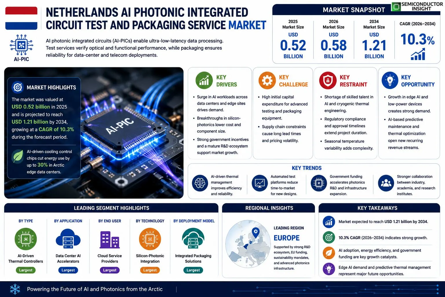
MARKET DRIVERS
Rising AI Compute Demand
Netherlands AI Photonic Integrated Circuit Test and Packaging Service Market is being propelled by a surge in AI‑driven workloads across data‑center and edge computing environments. Companies are seeking higher bandwidth and lower latency, which photonic solutions can provide, creating a steady pipeline of test and packaging contracts.
Advancements in Photonic Integration
Recent breakthroughs in silicon‑photonic platforms have reduced component size and cost, enabling broader adoption of AI‑optimized circuits. This technical progress translates directly into increased demand for specialized testing and high‑precision packaging services in the Dutch market.
➤ “The convergence of AI algorithms and photonic integration is reshaping the European semiconductor landscape, with the Netherlands emerging as a hub for advanced test services.”
Furthermore, strong government incentives for high‑tech manufacturing and a mature research ecosystem support the growth of Netherlands AI Photonic Integrated Circuit Test and Packaging Service Market, encouraging both domestic and foreign investment.
MARKET CHALLENGES
Complexity of Multi‑Channel Testing
Testing photonic circuits that support AI workloads often involves multi‑wavelength, high‑speed measurements. The required equipment is capital‑intensive, and skilled personnel are scarce, posing a barrier for smaller service providers.
Other Challenges
Regulatory Compliance
EU‑wide environmental and safety regulations add layers of certification that can extend time‑to‑market for new packaging solutions.Supply‑chain volatility, especially for specialty optical components, further complicates scheduling and cost management for service operators.
MARKET RESTRAINTS
High Capital Expenditure
Establishing state‑of‑the‑art test labs and clean‑room packaging facilities demands multi‑million‑euro investments, limiting entry to well‑funded incumbents and deterring new entrants.
Talent Shortage
The Netherlands faces a shortage of engineers with combined expertise in AI algorithms, photonic design, and high‑precision metrology, which restrains the speed at which service capacity can expand.Additionally, fragmented customer requirements across telecom, automotive, and data‑center sectors create customization challenges that can affect economies of scale.
MARKET OPPORTUNITIES
Growth of AI‑Accelerated Edge Devices
Edge deployments for autonomous vehicles and smart sensors are increasingly integrating photonic chips to meet power‑efficiency goals. This creates a niche for specialized test and packaging services that can handle ruggedized, low‑power designs.
Collaboration with Academic Institutes
Partnerships between service firms and Dutch universities enable access to cutting‑edge research, accelerating the development of test methodologies tailored for AI‑centric photonic circuits.Finally, the Dutch government’s strategic roadmap for quantum‑ready photonic infrastructure opens long‑term opportunities for service providers to expand into emerging quantum communication testing and packaging.
Netherlands AI Photonic Integrated Circuit Test and Packaging Service Market Trends
Government Funding Boosts Test and Packaging Capabilities
The Netherlands has earmarked €300 million through the Dutch Top Sector Photonics programme to accelerate research, development, and production of silicon‑photonics technologies. This capital injection is directed toward expanding clean‑room space, acquiring next‑generation optical test equipment, and establishing dedicated training centres for skilled technicians. Service providers report a measurable improvement in prototype validation cycles, with time‑to‑first‑silicon decreasing by roughly one‑fifth while still meeting the rigorous reliability standards required by cloud‑data‑center and telecom operators. The funding also encourages collaboration between universities and industry, fostering a pipeline of expertise that underpins Netherlands AI Photonic Integrated Circuit Test and Packaging Service Market’s ability to scale efficiently.
Other Trends
Automation of Wafer‑Level Testing
Recent advances in wafer‑level testing platforms integrate AI‑driven analytics that continuously monitor optical loss, bandwidth, and power consumption across entire wafers. By automating data capture and employing machine‑learning models to flag out‑of‑spec devices in real time, providers reduce manual inspection steps and lower overall testing costs. The enhanced precisionoften below sub‑nanometer tolerancessupports high‑volume manufacturing and shortens the feedback loop between design and production. This automation trend not only improves yield but also aligns with the broader European push toward fully digitalized photonic fabs, ensuring that testing and packaging services remain agile and competitive.
Strategic Partnerships Expand Service Portfolio
Key industry players such as LioniX International, ASML Holding, and Foundries have formed joint ventures and collaborative service lines within the Dutch ecosystem. These alliances combine ASML’s advanced lithography expertise with LioniX’s specialised packaging know‑how, delivering end‑to‑end solutions that integrate fiber‑coupled modules, multi‑chip assemblies, and robust thermal management. The coordinated approach enhances supply‑chain resilience, shortens lead times for custom AI‑PIC solutions, and positions the Netherlands as a preferred hub for Netherlands AI Photonic Integrated Circuit Test and Packaging Service Market. Multinational cloud providers and telecom operators are increasingly sourcing their high‑performance photonic modules from this integrated network, attracted by the consistent quality, rapid iteration capabilities, and proximity to European R&D centres.
COMPETITIVE LANDSCAPE
Key Industry Players
Netherlands AI Photonic Integrated Circuit Test and Packaging Service Market Overview
The Netherlands has emerged as a focal point for AI‑photonic integrated circuit (AI‑PIC) test and packaging services, driven by substantial public investment and a dense ecosystem of semiconductor manufacturers. LioniX International leads the market by providing wafer‑level testing platforms that evaluate optical loss, bandwidth, and power consumption, while its close collaboration with ASML ensures that the latest lithography tools are leveraged for high‑volume production. Foundries’ Dutch fab offers a vertically integrated offering, combining silicon‑photonic wafer fabrication with advanced test‑and‑pack modules that meet data‑center reliability standards, positioning it as a dominant player in the regional supply chain.Beyond the dominant trio, a cluster of niche innovators strengthens the competitive landscape. NXP Semiconductors contributes extensive electronic‑control expertise that complements photonic testing workflows, whereas Philips’ health‑technology division applies AI‑PIC packaging for high‑precision imaging sensors. TNO, the Dutch research organization, supplies independent validation services that certify module performance against European standards. Emerging spin‑offs such as Cycleo and MESA Imaging focus on specialized fiber‑coupled packaging, while international firms like IMEC (Belgium) and Silicon Valley‑based SiQuint maintain collaborative R&D ties with Dutch laboratories, expanding the pool of capable service providers.
List of Key Photonic Integrated Circuit Test and Packaging Service Companies Profiled
- LioniX International
- ASML Holding
- Foundries Netherlands
- NXP Semiconductors
- Philips Healthcare
- TNO (Netherlands Organisation for Applied Scientific Research)
- Cycleo (Eindhoven University spin‑off)
- MESA Imaging
- IMEC (European partner)
- SiQuint (now part of Foundries)
- Trinity Photonics
- Eurofins Scientific
- Vanguard Photonics
- CNM (Center for Nanoscience and Molecular) Netherlands
Segment Analysis:
| Segment Category | Sub-Segments | Key Insights |
| By Type |
|
Wafer‑level test services are the predominant focus in the Dutch market because they enable early defect detection and accelerate time‑to‑market for AI‑PIC designs.
|
| By Application |
|
Data‑center interconnect drives the strongest demand for AI‑PIC test and packaging services in the Netherlands.
|
| By End User |
|
Cloud service providers emerge as the leading end‑user segment, leveraging AI‑PICs to boost computational efficiency.
|
| By Testing Technology |
|
Machine‑learning‑driven fault detection is gaining traction as a differentiator for Dutch test service providers.
|
| By Service Model |
|
Managed testing‑as‑a‑service is emerging as the most attractive model for mid‑size AI‑PIC designers.
|
Regional Analysis: Netherlands AI Photonic Integrated Circuit Test and Packaging Service Market
Europe
The convergence of AI‑enabled network analytics and high‑performance photonic components fuels demand for sophisticated test services. Telecom operators pursuing 5G and beyond rely on integrated circuits that can process massive data streams, prompting service providers to specialize in AI‑augmented test suites that guarantee speed and reliability.
European standards such as EN 50173 and upcoming AI transparency regulations shape testing protocols. Providers must align packaging processes with safety and data‑privacy requirements, ensuring that AI‑driven diagnostics meet both performance and compliance benchmarks across member states.
A handful of niche firms dominate the European market, leveraging strong ties to research institutions. Partnerships between Dutch test labs and German equipment manufacturers create collaborative ecosystems that accelerate technology transfer and sustain competitive advantage.
North America
North America showcases a vibrant venture‑backed ecosystem that emphasizes rapid prototyping of AI‑enhanced photonic chips. While the United States does not host Netherlands AI Photonic Integrated Circuit Test and Packaging Service Market directly, its leading semiconductor foundries provide a benchmark for high‑volume testing capabilities. Companies in Silicon Valley are integrating AI models to predict failure modes, thereby shortening time‑to‑market. The region’s focus on data‑center expansion and edge computing drives demand for scalable PIC testing, encouraging service firms to adopt modular packaging solutions that can be customized for diverse applications.
Asia‑Pacific
The Asia‑Pacific region, led by China, Japan, and South Korea, is accelerating its photonic research agenda through substantial government funding. Although the Netherlands market remains European‑centric, Asian firms are closely watching AI‑driven test methodologies to enhance their own manufacturing pipelines. The rapid rollout of 5G infrastructure across the region creates a sizable need for high‑performance PICs, prompting local service providers to explore collaborations with European experts. Cultural emphasis on cost‑effective scaling also pushes the development of automated packaging lines that can handle large batches without compromising precision.
South America
South America’s telecom sector is undergoing modernization, with Brazil and Chile investing in fiber‑optic networks. The region’s emerging interest in AI‑powered network optimization makes it a prospective market for specialized PIC testing services. However, limited local manufacturing capacity means most test and packaging needs are outsourced to established European providers, including those in the Netherlands market. Partnerships focusing on knowledge transfer and remote AI analytics are emerging as key pathways to bridge the capability gap.
Middle East & Africa
In the Middle East and Africa, infrastructure projects such as smart city initiatives and expanding data‑center footprints generate nascent demand for advanced photonic solutions. While Netherlands AI Photonic Integrated Circuit Test and Packaging Service Market is still peripheral in this region, multinational service firms are establishing regional hubs to support local operators. Emphasis on reliability and energy efficiency aligns with regional sustainability goals, encouraging the adoption of AI‑guided test protocols that can assure performance under harsh environmental conditions.
Report Scope
This market research report provides a comprehensive analysis of the Netherlands AI Photonic Integrated Circuit Test and Packaging Service Market , covering the forecast period 2026–2034. It offers detailed insights into market dynamics, technological advancements, competitive landscape, and key trends shaping the industry.
Key focus areas of the report include:
- Market Overview: The report begins with an overview outlining its current market scenario, key growth indicators, and industry transformation drivers. It discusses macroeconomic factors, demand–supply balance, regulatory landscape, and the strategic role of semiconductors in powering advancements across industries such as automotive, telecommunications, consumer electronics, and industrial automation.
- Market Size & Forecast: Historical data and future projections for revenue, unit shipments, and market value across major regions and segments.
- Segmentation Analysis: Detailed breakdown by product type, technology, application, and end-user industry to identify high-growth segments and investment opportunities.
- Regional Insights: Insights into market performance across North America, Europe, Asia-Pacific, Latin America, and the Middle East & Africa, including country-level analysis where relevant.
- Competitive Landscape: Profiles of leading market participants, including their product offerings, R&D focus, manufacturing capacity, pricing strategies, and recent developments such as mergers, acquisitions, and partnerships.
- Technology Trends & Innovation: Assessment of emerging technologies, integration of AI/IoT, semiconductor design trends, fabrication techniques, and evolving industry standards.
- Market Drivers & Restraints: Evaluation of factors driving market growth along with challenges, supply chain constraints, regulatory issues, and market-entry barriers.
- Stakeholder Insights: Insights for component suppliers, OEMs, system integrators, investors, and policymakers regarding the evolving ecosystem and strategic opportunities.
Primary and secondary research methods are employed, including interviews with industry experts, data from verified sources, and real-time market intelligence to ensure the accuracy and reliability of the insights presented.
FREQUENTLY ASKED QUESTIONS:
What is the current market size of Netherlands AI Photonic Integrated Circuit Test and Packaging Service Market?
-> Netherlands AI Photonic Integrated Circuit Test and Packaging Service Market was valued at USD 0.52 billion in 2025 and is expected to reach USD 1.21 billion by 2034.
Which key companies operate in Netherlands AI Photonic Integrated Circuit Test and Packaging Service Market?
-> Key players include Axalta Coating Systems, AkzoNobel, BASF SE, PPG, Sherwin-Williams, and 3M, among others.
What are the key growth drivers?
-> Key growth drivers include railway infrastructure investments, urbanization, and demand for durable coatings.
Which region dominates the market?
-> Asia-Pacific is the fastest-growing region, while Europe remains a dominant market.
What are the emerging trends?
-> Emerging trends include bio-based coatings, smart coatings, and sustainable rail solutions.
Get Sample Report PDF for Exclusive Insights
Report Sample Includes
- Table of Contents
- List of Tables & Figures
- Charts, Research Methodology, and more...


