Key Statistics
Key Takeaways
- Market scale: The multi-chip package GaN chips market reached USD 737 million in 2025 and is projected at USD 1,758 million in 2034, representing a 10.1% compound annual expansion over 2026–2034. Integration of switches with driver, control and protection functions changes both component count and board-level qualification.
- Package configuration: Controller+Driver+GaN held a modeled ~37% of 2025 value, ahead of Driver+GaN at ~28%, Driver+2*GaN at ~22% and Driver+Protection+GaN at ~13%. Integrated half-bridge products can reduce layout complexity, while discrete alternatives remain appropriate where thermal or gate-drive independence is essential.
- Application mix: Industrial Power Supply accounted for a modeled ~32% of demand, followed by Electronic Vehicle Charger at ~25%, Electronic Equipment at ~21%, Communication Equipment at ~15% and Others at ~7%. Adoption depends on verified switching losses, electromagnetic compatibility and lifetime economics.
- Regional leadership: Asia-Pacific represented a modeled ~48% share, reflecting power-adapter production, electronics manufacturing and expanding GaN fabrication ecosystems. North America held ~23%, Europe ~20%, Middle East & Africa ~5% and South America ~4%, with different qualification and procurement channels.
- Technology direction: The 650V Class represented ~74% of modeled 2025 sales, while Medium Power led power rating at ~48%. Suppliers compete on integrating drivers without sacrificing fault protection, thermal resistance, assembly yield or predictable operation in demanding industrial environments.
Multi-chip Package GaN Chips Market Overview
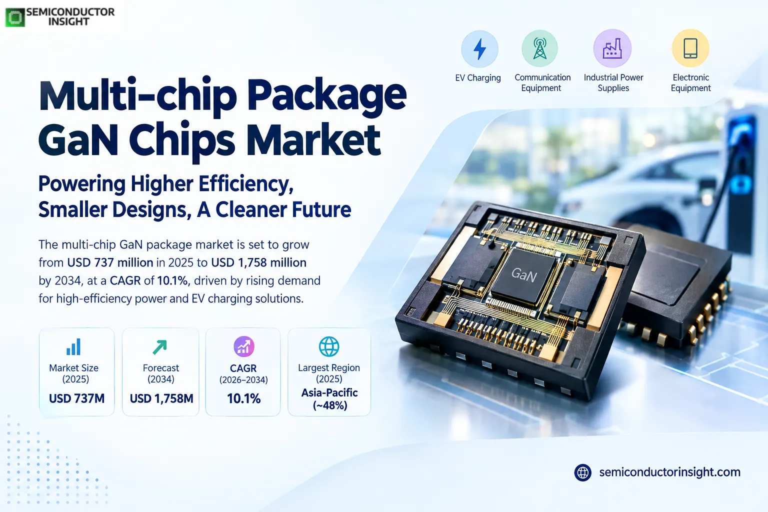
Multi-chip package GaN chips market reached USD 737 million in 2025 and is projected to attain USD 1,758 million by 2034, at a CAGR of 10.1% during 2026–2034. The market covers integrated GaN power semiconductor packages combining switching die with driver, control or protection functions, with Asia-Pacific holding the largest modeled regional share of ~48%.
A multi-chip GaN power package brings switching elements and at least one associated silicon or compound-semiconductor control function into a coordinated physical assembly. In a half bridge, two power switches share a carefully controlled layout with high-side and low-side drive circuitry; other packages combine one GaN device with protection or controller functions. This architecture is attractive where fast edges create parasitic inductance, but it also places demanding thermal and test requirements on packaging design, interconnect quality and final electrical screening.
Revenue includes GaN-containing multi-die semiconductor packages sold for electronic equipment, communication equipment, electric vehicle charging and industrial power supplies. The boundary excludes merchant GaN wafers, single-die discrete switches sold without the integrated package functions, RF-only power amplifiers and revenue from finished chargers, complete inverters or entire power supplies. Silicon driver and protection die remain within scope when they are assembled alongside GaN power switches, because that combination is a defining part of the packaged product rather than a separate downstream system.
The manufacturing problem is not simply to place more die under a common lid. Gate-loop inductance, dead-time control, common-mode noise, isolation spacing and heat flow must be validated across the complete switching envelope. A 650 V half-bridge package may remove external components and shorten a customer layout, yet its qualification must still cover short-circuit events, board assembly variation and the operating temperatures encountered in industrial equipment. These engineering costs create a premium for designs with reproducible performance rather than for package miniaturization alone.
Commercial traction is visible in several product families. Infineon described CoolGaN Drive HB 600 V G5 in February 2026 as a package combining two GaN switches, two gate-drive paths and a bootstrap diode. STMicroelectronics offers MasterGaN integrated half bridges, while Texas Instruments lists the LMG2100 integrated half-bridge platform. These examples establish the existence of the package architecture, but they do not imply that every GaN transistor or every system marketed by those companies belongs to the multi-chip package revenue pool.
The 2025 demand structure is modeled around six commercial lenses: region, package type, application, end-user industry, voltage rating and power rating. Each lens divides the same revenue boundary rather than describing additive markets. Higher-frequency switching can shrink magnetic components and improve conversion density, but realized demand depends on a supplier being designed into a repeatable bill of materials and maintaining quality through several product revisions. That qualification cycle explains why semiconductor package revenue grows more steadily than headline announcements about entire end-market installations.
Segment Analysis: By Type
Controller+Driver+GaN accounted for a modeled ~37% of 2025 package revenue. The category includes four integrated configurations, each distinguished by the combination of GaN switching and companion control die. Half-bridge and protection-integrated products address different customer pain points, so their price per package should not be treated as interchangeable. During the 2026–2034 outlook, commercial positioning depends on 650 V and 900 V product availability, qualification discipline and assembly economics rather than a single laboratory efficiency measurement. The 2025 modeled split is ~37%, ~28%, ~22% and ~13%, respectively. A successful design-in must also survive high-volume board assembly, supply continuity reviews and the customer’s thermal margin requirements before the revenue opportunity becomes repeatable.
| Package type | Engineering function | Commercial position |
|---|---|---|
| Controller+Driver+GaN | The integrated package accounted for a modeled ~37% of 2025 package revenue. This architecture couples control logic and gate-drive functions to GaN switching devices, reducing the external control bill of materials in compact converters. It is attractive in industrial supplies with closely controlled switching waveforms and in platforms seeking repeatable factory calibration. For Asia-Pacific Electronic Equipment Controller+Driver+GaN designs, during the 2026–2034 outlook, commercial positioning depends on 650 V and 900 V product availability, qualification discipline and assembly economics rather than a single laboratory efficiency measurement. Integrated control can simplify protection coordination, but customers still evaluate firmware interactions and failure behavior. For North America Electronic Equipment Controller+Driver+GaN designs, a successful design-in must also survive high-volume board assembly, supply continuity reviews and the customer’s thermal margin requirements before the revenue opportunity becomes repeatable. | This configuration accounted for a modeled ~37% of 2025 package revenue. For Europe Electronic Equipment Controller+Driver+GaN designs, integrated control can simplify protection coordination, but customers still evaluate firmware interactions and failure behavior. For Middle East & Africa Electronic Equipment Controller+Driver+GaN designs, this architecture couples control logic and gate-drive functions to GaN switching devices, reducing the external control bill of materials in compact converters. For South America Electronic Equipment Controller+Driver+GaN designs, during the 2026–2034 outlook, commercial positioning depends on 650 V and 900 V product availability, qualification discipline and assembly economics rather than a single laboratory efficiency measurement. For Asia-Pacific Communication Equipment Controller+Driver+GaN designs, it is attractive in industrial supplies with closely controlled switching waveforms and in platforms seeking repeatable factory calibration. For North America Communication Equipment Controller+Driver+GaN designs, a successful design-in must also survive high-volume board assembly, supply continuity reviews and the customer’s thermal margin requirements before the revenue opportunity becomes repeatable. |
| Driver+GaN | The integrated package accounted for a modeled ~28% of 2025 package revenue. The package places a dedicated driver close to the GaN switch to reduce parasitic gate-loop inductance and accelerate layout work. Power adapters and equipment manufacturers value the smaller footprint when board area is constrained, especially where high switching speed is necessary. For Europe Communication Equipment Controller+Driver+GaN designs, during the 2026–2034 outlook, commercial positioning depends on 650 V and 900 V product availability, qualification discipline and assembly economics rather than a single laboratory efficiency measurement. A single-switch integrated drive package may be less complex than a complete half bridge, with distinct heat-spreading constraints. For Middle East & Africa Communication Equipment Controller+Driver+GaN designs, a successful design-in must also survive high-volume board assembly, supply continuity reviews and the customer’s thermal margin requirements before the revenue opportunity becomes repeatable. | This configuration accounted for a modeled ~28% of 2025 package revenue. For South America Communication Equipment Controller+Driver+GaN designs, a single-switch integrated drive package may be less complex than a complete half bridge, with distinct heat-spreading constraints. For Asia-Pacific Electronic Vehicle Charger Controller+Driver+GaN designs, the package places a dedicated driver close to the GaN switch to reduce parasitic gate-loop inductance and accelerate layout work. For North America Electronic Vehicle Charger Controller+Driver+GaN designs, during the 2026–2034 outlook, commercial positioning depends on 650 V and 900 V product availability, qualification discipline and assembly economics rather than a single laboratory efficiency measurement. For Europe Electronic Vehicle Charger Controller+Driver+GaN designs, power adapters and equipment manufacturers value the smaller footprint when board area is constrained, especially where high switching speed is necessary. For Middle East & Africa Electronic Vehicle Charger Controller+Driver+GaN designs, a successful design-in must also survive high-volume board assembly, supply continuity reviews and the customer’s thermal margin requirements before the revenue opportunity becomes repeatable. |
| Driver+2*GaN | The integrated package accounted for a modeled ~22% of 2025 package revenue. Two GaN switches and their high-side and low-side gate drive form a compact half-bridge building block for power conversion. ST MasterGaN and Infineon CoolGaN Drive HB demonstrate how the physical integration can support synchronous power stages. For South America Electronic Vehicle Charger Controller+Driver+GaN designs, during the 2026–2034 outlook, commercial positioning depends on 650 V and 900 V product availability, qualification discipline and assembly economics rather than a single laboratory efficiency measurement. Switch matching and dead-time control become central tests, particularly when the package faces repetitive high-frequency transients. For Asia-Pacific Industrial Power Supply Controller+Driver+GaN designs, a successful design-in must also survive high-volume board assembly, supply continuity reviews and the customer’s thermal margin requirements before the revenue opportunity becomes repeatable. | This configuration accounted for a modeled ~22% of 2025 package revenue. For North America Industrial Power Supply Controller+Driver+GaN designs, switch matching and dead-time control become central tests, particularly when the package faces repetitive high-frequency transients. For Europe Industrial Power Supply Controller+Driver+GaN designs, two GaN switches and their high-side and low-side gate drive form a compact half-bridge building block for power conversion. For Middle East & Africa Industrial Power Supply Controller+Driver+GaN designs, during the 2026–2034 outlook, commercial positioning depends on 650 V and 900 V product availability, qualification discipline and assembly economics rather than a single laboratory efficiency measurement. For South America Industrial Power Supply Controller+Driver+GaN designs, sT MasterGaN and Infineon CoolGaN Drive HB demonstrate how the physical integration can support synchronous power stages. For Asia-Pacific Others Controller+Driver+GaN designs, a successful design-in must also survive high-volume board assembly, supply continuity reviews and the customer’s thermal margin requirements before the revenue opportunity becomes repeatable. |
| Driver+Protection+GaN | The integrated package accounted for a modeled ~13% of 2025 package revenue. Protection circuitry complements the switching device and its driver through overcurrent sensing or fault-handling functions. Applications with expensive downstream electronics may pay for integrated protection rather than add external circuits on a crowded board. For North America Others Controller+Driver+GaN designs, during the 2026–2034 outlook, commercial positioning depends on 650 V and 900 V product availability, qualification discipline and assembly economics rather than a single laboratory efficiency measurement. Qualification focuses on response time, fault recovery and the behavior of sensing circuits at elevated temperature. For Europe Others Controller+Driver+GaN designs, a successful design-in must also survive high-volume board assembly, supply continuity reviews and the customer’s thermal margin requirements before the revenue opportunity becomes repeatable. | This configuration accounted for a modeled ~13% of 2025 package revenue. For Middle East & Africa Others Controller+Driver+GaN designs, qualification focuses on response time, fault recovery and the behavior of sensing circuits at elevated temperature. For South America Others Controller+Driver+GaN designs, protection circuitry complements the switching device and its driver through overcurrent sensing or fault-handling functions. For Asia-Pacific Electronic Equipment Driver+GaN designs, during the 2026–2034 outlook, commercial positioning depends on 650 V and 900 V product availability, qualification discipline and assembly economics rather than a single laboratory efficiency measurement. For North America Electronic Equipment Driver+GaN designs, applications with expensive downstream electronics may pay for integrated protection rather than add external circuits on a crowded board. For Europe Electronic Equipment Driver+GaN designs, a successful design-in must also survive high-volume board assembly, supply continuity reviews and the customer’s thermal margin requirements before the revenue opportunity becomes repeatable. |
Controller+Driver+GaN
Controller+Driver+GaN accounted for a modeled ~37% of 2025 package revenue. For Middle East & Africa Electronic Equipment Driver+GaN designs, this architecture couples control logic and gate-drive functions to GaN switching devices, reducing the external control bill of materials in compact converters. For South America Electronic Equipment Driver+GaN designs, it is attractive in industrial supplies with closely controlled switching waveforms and in platforms seeking repeatable factory calibration. For Asia-Pacific Communication Equipment Driver+GaN designs, during the 2026–2034 outlook, commercial positioning depends on 650 V and 900 V product availability, qualification discipline and assembly economics rather than a single laboratory efficiency measurement. For North America Communication Equipment Driver+GaN designs, integrated control can simplify protection coordination, but customers still evaluate firmware interactions and failure behavior. For Europe Communication Equipment Driver+GaN designs, a successful design-in must also survive high-volume board assembly, supply continuity reviews and the customer’s thermal margin requirements before the revenue opportunity becomes repeatable.
Driver+GaN
Driver+GaN accounted for a modeled ~28% of 2025 package revenue. For Middle East & Africa Communication Equipment Driver+GaN designs, the package places a dedicated driver close to the GaN switch to reduce parasitic gate-loop inductance and accelerate layout work. For South America Communication Equipment Driver+GaN designs, power adapters and equipment manufacturers value the smaller footprint when board area is constrained, especially where high switching speed is necessary. For Asia-Pacific Electronic Vehicle Charger Driver+GaN designs, during the 2026–2034 outlook, commercial positioning depends on 650 V and 900 V product availability, qualification discipline and assembly economics rather than a single laboratory efficiency measurement. For North America Electronic Vehicle Charger Driver+GaN designs, a single-switch integrated drive package may be less complex than a complete half bridge, with distinct heat-spreading constraints. For Europe Electronic Vehicle Charger Driver+GaN designs, a successful design-in must also survive high-volume board assembly, supply continuity reviews and the customer’s thermal margin requirements before the revenue opportunity becomes repeatable.
Driver+2*GaN
Driver+2*GaN accounted for a modeled ~22% of 2025 package revenue. For Middle East & Africa Electronic Vehicle Charger Driver+GaN designs, two GaN switches and their high-side and low-side gate drive form a compact half-bridge building block for power conversion. For South America Electronic Vehicle Charger Driver+GaN designs, sT MasterGaN and Infineon CoolGaN Drive HB demonstrate how the physical integration can support synchronous power stages. For Asia-Pacific Industrial Power Supply Driver+GaN designs, during the 2026–2034 outlook, commercial positioning depends on 650 V and 900 V product availability, qualification discipline and assembly economics rather than a single laboratory efficiency measurement. For North America Industrial Power Supply Driver+GaN designs, switch matching and dead-time control become central tests, particularly when the package faces repetitive high-frequency transients. For Europe Industrial Power Supply Driver+GaN designs, a successful design-in must also survive high-volume board assembly, supply continuity reviews and the customer’s thermal margin requirements before the revenue opportunity becomes repeatable.
Driver+Protection+GaN
Driver+Protection+GaN accounted for a modeled ~13% of 2025 package revenue. For Middle East & Africa Industrial Power Supply Driver+GaN designs, protection circuitry complements the switching device and its driver through overcurrent sensing or fault-handling functions. For South America Industrial Power Supply Driver+GaN designs, applications with expensive downstream electronics may pay for integrated protection rather than add external circuits on a crowded board. For Asia-Pacific Others Driver+GaN designs, during the 2026–2034 outlook, commercial positioning depends on 650 V and 900 V product availability, qualification discipline and assembly economics rather than a single laboratory efficiency measurement. For North America Others Driver+GaN designs, qualification focuses on response time, fault recovery and the behavior of sensing circuits at elevated temperature. For Europe Others Driver+GaN designs, a successful design-in must also survive high-volume board assembly, supply continuity reviews and the customer’s thermal margin requirements before the revenue opportunity becomes repeatable.
Segment Analysis: By Application
Industrial Power Supply accounted for a modeled ~32% of 2025 package revenue. Applications are allocated by the finished equipment into which a GaN multi-chip package is sold, without adding the value of that equipment. Industrial supplies and charging stages dominate engineering attention, while communication and electronic equipment provide a diversified customer base. For Middle East & Africa Others Driver+GaN designs, during the 2026–2034 outlook, commercial positioning depends on 650 V and 900 V product availability, qualification discipline and assembly economics rather than a single laboratory efficiency measurement. The application shares are ~32%, ~25%, ~21%, ~15% and ~7% in the modeled base year. For South America Others Driver+GaN designs, a successful design-in must also survive high-volume board assembly, supply continuity reviews and the customer’s thermal margin requirements before the revenue opportunity becomes repeatable.
| Application | Demand characteristics |
|---|---|
| Electronic Equipment | Electronic Equipment accounted for a modeled ~21% of 2025 package revenue. Use cases include compact notebook power supplies, adapters and specialized electronics. Designers favor predictable board footprint, switching efficiency and manageable electromagnetic emissions. The value case improves when an integrated package removes enough surrounding components to offset its semiconductor premium. For Asia-Pacific Electronic Equipment Driver+2*GaN designs, during the 2026–2034 outlook, commercial positioning depends on 650 V and 900 V product availability, qualification discipline and assembly economics rather than a single laboratory efficiency measurement. The distinction is a semiconductor package socket rather than finished equipment revenue. For North America Electronic Equipment Driver+2*GaN designs, a successful design-in must also survive high-volume board assembly, supply continuity reviews and the customer’s thermal margin requirements before the revenue opportunity becomes repeatable. |
| Communication Equipment | Communication Equipment accounted for a modeled ~15% of 2025 package revenue. Use cases include telecommunications rectifiers, network power cards and supporting infrastructure. Equipment vendors often require long availability commitments and controlled electrical behavior across temperature. Higher system uptime and qualified redundancy matter more than a small improvement in laboratory peak efficiency. For Europe Electronic Equipment Driver+2*GaN designs, during the 2026–2034 outlook, commercial positioning depends on 650 V and 900 V product availability, qualification discipline and assembly economics rather than a single laboratory efficiency measurement. For Middle East & Africa Electronic Equipment Driver+2*GaN designs, the distinction is a semiconductor package socket rather than finished equipment revenue. For South America Electronic Equipment Driver+2*GaN designs, a successful design-in must also survive high-volume board assembly, supply continuity reviews and the customer’s thermal margin requirements before the revenue opportunity becomes repeatable. |
| Electronic Vehicle Charger | Electronic Vehicle Charger accounted for a modeled ~25% of 2025 package revenue. Use cases include onboard charging stages and selected vehicle-related power conversion. Automotive and charging designers assess reliability, isolation, transients and compatibility with higher-voltage architectures. Automotive qualification may extend the sales cycle even when power-density benefits appear compelling. For Asia-Pacific Communication Equipment Driver+2*GaN designs, during the 2026–2034 outlook, commercial positioning depends on 650 V and 900 V product availability, qualification discipline and assembly economics rather than a single laboratory efficiency measurement. For North America Communication Equipment Driver+2*GaN designs, the distinction is a semiconductor package socket rather than finished equipment revenue. For Europe Communication Equipment Driver+2*GaN designs, a successful design-in must also survive high-volume board assembly, supply continuity reviews and the customer’s thermal margin requirements before the revenue opportunity becomes repeatable. |
| Industrial Power Supply | For Middle East & Africa Communication Equipment Driver+2*GaN designs, industrial Power Supply accounted for a modeled ~32% of 2025 package revenue. Use cases include industrial AC/DC, DC/DC and power-distribution assemblies. Industrial users prize service life, component availability and reproducible high-frequency switching under variable load. This modeled leading application is supported by broad integrated-GaN product positioning and industrial reference designs. For South America Communication Equipment Driver+2*GaN designs, during the 2026–2034 outlook, commercial positioning depends on 650 V and 900 V product availability, qualification discipline and assembly economics rather than a single laboratory efficiency measurement. For Asia-Pacific Electronic Vehicle Charger Driver+2*GaN designs, the distinction is a semiconductor package socket rather than finished equipment revenue. For North America Electronic Vehicle Charger Driver+2*GaN designs, a successful design-in must also survive high-volume board assembly, supply continuity reviews and the customer’s thermal margin requirements before the revenue opportunity becomes repeatable. |
| Others | Others accounted for a modeled ~7% of 2025 package revenue. Use cases include specialized laboratory, energy and low-volume embedded equipment. These use cases often involve limited runs, custom magnetic components and engineering-led purchasing rather than commodity production. A small revenue contribution can still support technically demanding niche packages and reference designs. For Europe Electronic Vehicle Charger Driver+2*GaN designs, during the 2026–2034 outlook, commercial positioning depends on 650 V and 900 V product availability, qualification discipline and assembly economics rather than a single laboratory efficiency measurement. For Middle East & Africa Electronic Vehicle Charger Driver+2*GaN designs, the distinction is a semiconductor package socket rather than finished equipment revenue. For South America Electronic Vehicle Charger Driver+2*GaN designs, a successful design-in must also survive high-volume board assembly, supply continuity reviews and the customer’s thermal margin requirements before the revenue opportunity becomes repeatable. |
Industrial and charging design wins accounted for a modeled ~57% of 2025 package revenue. Industrial Power Supply and Electronic Vehicle Charger together form the principal addressable opportunity for higher-value integrated switches. Different qualification cycles mean the 2 categories should not be extrapolated from identical unit-growth assumptions. For Asia-Pacific Industrial Power Supply Driver+2*GaN designs, during the 2026–2034 outlook, commercial positioning depends on 650 V and 900 V product availability, qualification discipline and assembly economics rather than a single laboratory efficiency measurement. Industrial platforms may prioritize maintenance intervals while charging equipment puts particular emphasis on switching losses and packaging compactness. For North America Industrial Power Supply Driver+2*GaN designs, a successful design-in must also survive high-volume board assembly, supply continuity reviews and the customer’s thermal margin requirements before the revenue opportunity becomes repeatable.
Regional Analysis
Asia-Pacific accounted for a modeled ~48% of 2025 package revenue. Regional shares reflect where semiconductor packages are sold into equipment manufacturing and conversion-system assembly. Asia-Pacific leads due to its broad electronics supply chain, while North America and Europe provide substantial design and industrial demand. For Europe Industrial Power Supply Driver+2*GaN designs, during the 2026–2034 outlook, commercial positioning depends on 650 V and 900 V product availability, qualification discipline and assembly economics rather than a single laboratory efficiency measurement. The five modeled regional allocations total the same global 2025 package revenue, with estimated regional growth paths through 2034. For Middle East & Africa Industrial Power Supply Driver+2*GaN designs, a successful design-in must also survive high-volume board assembly, supply continuity reviews and the customer’s thermal margin requirements before the revenue opportunity becomes repeatable.
Where is the largest multi-chip GaN package market and how do regional requirements differ?
Asia-Pacific accounted for a modeled ~48% of 2025 package revenue. High-volume power-adapter and electronics assembly creates a broad qualification funnel for integrated GaN components. North America and Europe add industrial and vehicle-related power applications, whereas smaller regions often procure through finished power-system manufacturers. For South America Industrial Power Supply Driver+2*GaN designs, during the 2026–2034 outlook, commercial positioning depends on 650 V and 900 V product availability, qualification discipline and assembly economics rather than a single laboratory efficiency measurement. The regional view tracks the sale of GaN multi-chip packages, not national GaN wafer production capacity or complete charger shipment values. For Asia-Pacific Others Driver+2*GaN designs, a successful design-in must also survive high-volume board assembly, supply continuity reviews and the customer’s thermal margin requirements before the revenue opportunity becomes repeatable.
| Region | Position | Growth outlook | Demand profile | What decides supplier selection |
|---|---|---|---|---|
| Asia-Pacific | Modeled ~48% in 2025; largest revenue base. Regional outlook is ~10.9% CAGR across 2025–2034 as package qualification progresses. | GaN multi-chip package revenue reflects electronics assembly and power-device fabrication. Growth depends on adoption of 650 V integrated stages and on the timing of industrial customer design cycles, not the installed value of completed equipment. | Primary sockets are linked to electronics assembly and power-device fabrication, including products requiring careful gate-drive control, fault behavior and component lifetime. Local demand is sensitive to import channels and downstream electronics assembly. | Supplier selection emphasizes factory scale, assembly qualification and regional sourcing. Buyers also compare 900 V roadmaps, temperature qualification, assembly yield and support for 2026–2034 product revisions. |
| North America | Modeled ~23% in 2025; specialized revenue base. Regional outlook is ~9.0% CAGR across 2025–2034 as package qualification progresses. | GaN multi-chip package revenue reflects design-led data-center and industrial power electronics. For North America Others Driver+2*GaN designs, growth depends on adoption of 650 V integrated stages and on the timing of industrial customer design cycles, not the installed value of completed equipment. | Primary sockets are linked to design-led data-center and industrial power electronics, including products requiring careful gate-drive control, fault behavior and component lifetime. For Europe Others Driver+2*GaN designs, local demand is sensitive to import channels and downstream electronics assembly. | Supplier selection emphasizes engineering qualification and long-term product support. For Middle East & Africa Others Driver+2*GaN designs, buyers also compare 900 V roadmaps, temperature qualification, assembly yield and support for 2026–2034 product revisions. |
| Europe | Modeled ~20% in 2025; specialized revenue base. Regional outlook is ~9.1% CAGR across 2025–2034 as package qualification progresses. | GaN multi-chip package revenue reflects industrial power systems and automotive charging electronics. For South America Others Driver+2*GaN designs, growth depends on adoption of 650 V integrated stages and on the timing of industrial customer design cycles, not the installed value of completed equipment. | Primary sockets are linked to industrial power systems and automotive charging electronics, including products requiring careful gate-drive control, fault behavior and component lifetime. For Asia-Pacific Electronic Equipment Driver+Protection+GaN designs, local demand is sensitive to import channels and downstream electronics assembly. | Supplier selection emphasizes industrial certification and supply-chain traceability. For North America Electronic Equipment Driver+Protection+GaN designs, buyers also compare 900 V roadmaps, temperature qualification, assembly yield and support for 2026–2034 product revisions. |
| Middle East & Africa | Modeled ~5% in 2025; specialized revenue base. Regional outlook is ~11.2% CAGR across 2025–2034 as package qualification progresses. | GaN multi-chip package revenue reflects imported power-conversion assemblies for infrastructure. For Europe Electronic Equipment Driver+Protection+GaN designs, growth depends on adoption of 650 V integrated stages and on the timing of industrial customer design cycles, not the installed value of completed equipment. | Primary sockets are linked to imported power-conversion assemblies for infrastructure, including products requiring careful gate-drive control, fault behavior and component lifetime. For Middle East & Africa Electronic Equipment Driver+Protection+GaN designs, local demand is sensitive to import channels and downstream electronics assembly. | Supplier selection emphasizes distribution coverage, heat tolerance and project scheduling. For South America Electronic Equipment Driver+Protection+GaN designs, buyers also compare 900 V roadmaps, temperature qualification, assembly yield and support for 2026–2034 product revisions. |
| South America | Modeled ~4% in 2025; specialized revenue base. Regional outlook is ~10.3% CAGR across 2025–2034 as package qualification progresses. | GaN multi-chip package revenue reflects imported industrial power systems and charging equipment. For Asia-Pacific Communication Equipment Driver+Protection+GaN designs, growth depends on adoption of 650 V integrated stages and on the timing of industrial customer design cycles, not the installed value of completed equipment. | Primary sockets are linked to imported industrial power systems and charging equipment, including products requiring careful gate-drive control, fault behavior and component lifetime. For North America Communication Equipment Driver+Protection+GaN designs, local demand is sensitive to import channels and downstream electronics assembly. | Supplier selection emphasizes landed cost, distributor stock and currency exposure. For Europe Communication Equipment Driver+Protection+GaN designs, buyers also compare 900 V roadmaps, temperature qualification, assembly yield and support for 2026–2034 product revisions. |
Multi-chip Package GaN Chips Manufacturers and Competitive Landscape
Competitive differentiation in integrated GaN packages depends on whether suppliers combine transistor design, driver architecture, fault handling, package thermals and reference-design support. Infineon, STMicroelectronics and Texas Instruments have documented integrated power-stage products, while Power Integrations and Navitas demonstrate adjacent integration approaches. The broader manufacturer roster includes participants at different points in the semiconductor supply chain; inclusion does not establish that every company ships the same multi-die configuration.
Infineon expands its integrated GaN portfolio through CoolGaN Drive products that combine gate drivers with single switches or half bridges. The February 2026 Drive HB family explicitly integrates two 600 V GaN switches with high-side and low-side drive paths. This matters because reducing external gate-drive loop length can simplify a converter layout, yet thermal design and fault protection remain important competitive dimensions. Qualification evidence is stronger than an unsupported market-share ranking when comparing this architecture with alternative integrated solutions.
STMicroelectronics MasterGaN packages provide a second commercial reference point, with two high-voltage GaN transistors and driver functions combined inside one device family. Texas Instruments offers integrated half-bridge components such as LMG2100, showing that lower-voltage power stages can also use the package concept. The market therefore spans multiple voltage classes and application needs rather than a single 650 V charger category. Supplier differentiation turns on device behavior, package size, evaluation tools and support for the customer switching topology.
Power Integrations markets PowiGaN-enabled integrated power-conversion IC technology, while Navitas describes GaNFast power ICs that combine GaN switching with drive and related functions. These are relevant product ecosystems, but package architectures differ and not every integrated power IC necessarily contains the same die combination. Renesas completed its acquisition of Transphorm in June 2024; treating Transphorm as an independent 2026 company would misstate corporate ownership. Additional publisher-listed manufacturers warrant product-by-product qualification before being described as direct suppliers of specific multi-chip devices.
Pricing competition is affected by foundry process maturity, package assembly yield, electrical test coverage and the number of qualified second sources. A customer may prefer a proven 650 V integrated device over a more ambitious 1200 V roadmap when its operating voltage does not require the extra rating. At higher power levels, gate-driver isolation, protection behavior and thermal impedance can outweigh nominal die-area savings. These considerations support differentiated product strategies rather than a universal market concentration percentage.
Tier structure
| Tier | Companies | Basis of competition |
|---|---|---|
| Integrated half-bridge specialists | Infineon Technologies; STMicroelectronics; Texas Instruments | Public integrated GaN package portfolios support evaluation of switch count, driver arrangement and switching behavior. |
| Power IC and control integrators | Power Integrations; Navitas Semiconductor; Renesas Electronics | GaN power ICs and reference designs address compact conversion, with architecture-specific inclusion depending on the die combination. |
| Regional and ecosystem participants | Innoscience; Southchip Semiconductor; Kiwi Instruments; Chipown; DONGKE | Adjacent GaN, driver and power-management participation; individual multi-chip package availability requires product-level confirmation. |
Key companies profiled
- Infineon Technologies
- STMicroelectronics
- Texas Instruments
- Power Integrations
- Navitas Semiconductor
- Renesas Electronics
- Innoscience
- Southchip Semiconductor Technology
- Kiwi Instruments
- Chipown
- DONGKE
- HYSIC
- SPMICRO
- Wuxi SI-POWER MICRO-ELECTRONICS
Multi-chip Package GaN Chips Production and Capacity Analysis
Production combines GaN epitaxial and transistor fabrication, silicon control-die supply, assembly into thermally efficient packages and end-of-line electrical screening. The revenue opportunity is the qualified semiconductor package rather than wafer capacity itself. Manufacturing competitiveness depends on the ability to deliver stable switching behavior at volume, manage fast-edge electromagnetic effects and maintain traceability across more than one die technology in the same assembly.
The upstream flow begins with GaN transistor wafers and companion driver or protection silicon die, which may come from different process lines. Package engineers then design short current paths, heat-spreading structures and reliable interconnects before the product enters assembly and final test. Unlike a discrete switch, the integrated unit must be screened for interactions between the GaN stage and its drive functions. A defect in either component can compromise the entire package, making known-good-die handling and statistical process control commercially important.
Infineon and STMicroelectronics illustrate how product development spans semiconductor physics and application-level converter design. Their integrated GaN families are sold with evaluation information that helps customers characterize switching performance. That support is valuable because a compact package does not remove the need for board layout, electromagnetic interference testing or system thermal modeling. Customers also require continuity between package revisions so that a validated power supply can retain its electrical margins without repeating the full qualification process.
Manufacturing geography and demand geography need not match. Asia-Pacific has extensive electronics assembly and semiconductor packaging activity, while North American and European teams contribute architecture, industrial design and customer qualification. Package suppliers therefore balance cost, wafer availability, substrate compatibility and traceability across a distributed chain. The outlook through 2034 favors suppliers that can move from sample builds to stable multi-source logistics while maintaining driver timing, fault response and thermal performance across production lots.
Multi-chip Package GaN Chips Market Dynamics: Drivers, Restraints and Opportunities
Integrated GaN power stages benefit from smaller magnetic components, simplified board layout and the need for efficient industrial and charging conversion. Expansion is moderated by device cost, electromagnetic qualification and competing silicon or silicon-carbide designs. The following impact assessment distributes the reconciled forecast growth across concrete adoption forces and constraints rather than assigning the entire increase to one end-market indicator.
MARKET DRIVERS
Drivers Impact Analysis*
| Market Drivers | Impact Rank | CAGR Contribution (%) | 2026–2028 | 2029–2031 | 2032–2034 |
|---|---|---|---|---|---|
| Industrial power conversion and higher switching density | High | +5.00% | High | High | High |
| EV charger and onboard power-stage integration | High | +4.30% | Medium | High | High |
| Compact electronic equipment and adapters | Medium-High | +3.50% | High | Medium | Medium |
| Telecom and data-center power density requirements | Medium | +2.70% | Medium | High | High |
| Driver and protection integration reducing board complexity | Low-Medium | +1.90% | High | High | Medium |
| Others (evaluation ecosystems and improved package assembly) | Low | +1.40% | Medium | Medium | High |
Industrial conversion raises integrated power-stage demand
Industrial equipment designers increasingly compare package-level power density rather than only individual transistor switching losses. Integrating GaN switches with their driver circuits can shorten high-frequency loops and simplify a power-board layout, but a supplier still needs to demonstrate thermal endurance and protection behavior. This makes industrial power supplies a large modeled application for the 2025 base year. The 2026–2034 growth contribution reflects repeatable equipment designs and product refreshes rather than the entire value of industrial machinery.
Vehicle charging opens higher-value qualification pathways
Onboard and related electric-vehicle charging systems require efficient conversion in constrained spaces, encouraging evaluation of GaN integrated stages. Renesas has described automotive GaN reference designs following its Transphorm acquisition, while Navitas has discussed automotive-qualified GaN power ICs. Those developments are relevant demand signals, but they do not establish a one-to-one conversion of vehicle sales into multi-chip packages. Suppliers must meet switching, fault-response and supply-continuity requirements before commercial revenue scales.
Consumer adapters sustain a broad design funnel
Compact electronic equipment continues to motivate higher-frequency power conversion because magnetic components and heat management influence the size of a finished adapter. Integrated GaN power stages can reduce the number of external components in selected topologies, which is valuable when board area is constrained. The semiconductor package market captures only the device value, not the price of the adapter. As a result, product mix and qualification wins matter more than consumer unit counts alone.
Infrastructure power designs value density and serviceability
Telecommunications and data-center power supplies face pressure to deliver reliable power within fixed rack and enclosure dimensions. GaN devices are considered for selected conversion stages where switching speed and efficiency offer measurable benefits, while silicon and silicon carbide remain competitive in other voltage and power ranges. The opportunity for multi-chip packages depends on thermal margin, electromagnetic compatibility and long-life operation. A design win is most valuable when the customer standardizes the device across multiple product generations.
MARKET RESTRAINTS
Restraints Impact Analysis*
| Market Restraints | Impact Rank | CAGR Contribution (%) | 2026–2028 | 2029–2031 | 2032–2034 |
|---|---|---|---|---|---|
| High device and assembly cost versus silicon | High | -3.20% | High | Medium | Medium |
| Electromagnetic and thermal qualification burden | Medium-High | -2.40% | High | High | Medium |
| Competition from SiC and discrete GaN designs | Medium | -2.10% | Medium | High | High |
| Others (sourcing concentration and long design cycles) | Low | -1.00% | Medium | Medium | Low |
Package cost remains above mature silicon alternatives
A multi-die GaN package combines wafer processing, driver silicon, specialized assembly and more elaborate electrical screening. These costs can outweigh the value of fewer board components in price-sensitive equipment. Customers therefore evaluate the total converter bill of materials and thermal design rather than accept a device premium automatically. Price competition becomes more intense as suppliers improve yield and offer second sources, potentially reducing revenue growth even when package volumes increase.
Fast switching raises qualification complexity
GaN power stages can switch quickly enough to make parasitic inductance, electromagnetic interference and gate-drive timing critical system variables. Integration shortens some electrical paths but does not remove the need for board-level testing and protection coordination. In industrial and automotive environments, extended qualification schedules can delay conversion from engineering samples to recurring orders. Device makers that provide reliable evaluation boards and design support can reduce these delays, though they cannot eliminate them.
Alternative architectures retain attractive economics
Discrete GaN switches, silicon MOSFETs and SiC devices offer different trade-offs in voltage capability, cost and thermal design. Some customers prefer a separate driver to preserve flexibility, especially when the control strategy changes across product variants. Higher-voltage converter designs may favor SiC or established silicon modules instead of integrated GaN packages. Competitive substitution therefore limits the share of power-conversion spending that can be attributed to the multi-chip category.
Sourcing and redesign risks slow industrial adoption
Integrated devices combine multiple functions inside one package, making replacement with a second source more complicated than swapping a discrete transistor. Customers must compare pinout, protection timing, thermal impedance and electromagnetic behavior before approving a substitute. Longer equipment lifetimes increase the importance of supplier continuity and change notifications. Regional procurement restrictions and inventory cycles can compound this problem, particularly for buyers managing products across several geographic markets.
MARKET OPPORTUNITIES
Qualified 650 V half bridges for compact conversion
The largest modeled voltage class is 650 V, reflecting the widespread use of integrated GaN switching stages in AC/DC and related conversion. Suppliers that can combine two switches with dependable gate drive and accessible evaluation tools may shorten customer design time. The opportunity is strongest where switching frequency allows smaller passive components without excessive electromagnetic filtering. Volume growth depends on passing customer reliability gates and establishing repeat orders rather than on announcing additional prototype packages.
Advanced protection within the package
Adding sensing and protection functions can differentiate an integrated power stage when downstream equipment is expensive or safety critical. Protection timing must remain predictable during high-current events, and designers must understand the recovery behavior of the complete device. Vendors that document these characteristics can move beyond component-price competition. The resulting revenue opportunity comes from qualified packages with demonstrable system benefits, not from the value of complete protected power systems.
High-density telecom and computing power
Telecommunications rectifiers and computing power supplies create design opportunities for devices that reduce losses and footprint in selected conversion stages. Power Integrations and other GaN suppliers have described higher-voltage technology development, while mature 650 V products remain important for established designs. These announcements support a technology roadmap, not an assumption that every demonstrated high-voltage device is already shipping as a multi-chip package. Suppliers need credible thermal, assembly and reliability evidence to convert interest into volume.
Manufacturing consistency and evaluation platforms
A package vendor can improve its commercial position by providing application notes, reference boards and long-term component availability alongside its silicon and GaN integration. Such support lowers engineering risk for customers who would otherwise assemble drivers and switches from separate suppliers. Repeatable electrical test and known-good-die handling can improve yield and delivery reliability. The opportunity is particularly relevant to industrial customers seeking several years of unchanged performance across product revisions.
Multi-chip Package GaN Chips Supply Chain Analysis
The supply chain joins GaN transistor fabrication with silicon driver and controller manufacturing, advanced packaging, distribution and application engineering. Revenue is recognized at the integrated semiconductor package level. Because the component combines several functions, buyers must qualify both its power-switch behavior and the response of associated driver or protection circuits. Traceability and lifecycle management are important throughout the chain, especially for industrial and automotive-oriented applications.
Upstream semiconductor inputs. GaN switching die and companion silicon functions may be fabricated on different process nodes before integration. Suppliers must manage wafer yield, device screening and consistency of the driver interface. A package that passes transistor-level tests may still fail system-level electromagnetic or thermal requirements if its internal interconnect is poorly designed. The upstream value chain therefore includes electrical characterization and design support rather than only the cost of raw materials.
Assembly and electrical validation. Multi-die assembly places a premium on controlled bonding, heat flow and gate-loop geometry. Final test must assess both switching characteristics and integrated protection or drive functionality across specified temperature conditions. Package-level yield is especially sensitive to the quality of every included die, so known-good-die practices and robust process control influence delivered cost. Reliable production data can become a competitive advantage when customers move from sample orders to larger equipment platforms.
Commercial channels and design tools. Integrated GaN packages are often selected through application-engineering discussions and reference designs rather than simple commodity substitution. Distributors help small manufacturers obtain evaluation stock, while larger industrial customers negotiate qualification plans and lifecycle commitments directly. Vendor software, thermal models and board-layout guidance reduce integration risk. These services support semiconductor sales but are not counted as separate multi-chip package revenue unless included in the device transaction.
Downstream customer economics. The purchasing decision depends on the complete converter design, including magnetics, filtering, cooling and assembly. A more expensive integrated GaN device may lower total cost if it reduces passive components or improves efficiency, but that outcome is application specific. Industrial customers also weigh replacement risk and service lifetime, while consumer equipment makers prioritize space and high-volume cost. The package market therefore follows qualified component sockets rather than the total value of downstream systems.
Recent Developments in Multi-chip GaN Power Packaging
- 26 February 2026 Product launch
Infineon introduced the CoolGaN Drive HB 600 V G5 family with two GaN power switches, high-side and low-side drivers and a bootstrap diode in one package. This is direct evidence of an integrated half-bridge product architecture. Its commercial significance lies in fewer external gate-drive components and a shorter high-frequency current path, although converter-level electromagnetic and thermal verification remains necessary before a customer can move from an evaluation board to production. Source - 5 August 2026 Technology demonstration
Power Integrations announced a 2200 V PowiGaN technology demonstration for future high-voltage power systems. The announcement shows how GaN voltage capability is being extended toward demanding applications, but it does not establish that 2200 V multi-chip packages are shipping in volume. For the integrated-package market, the significance is a longer-term technology pathway that must still pass package assembly, fault-protection and customer qualification requirements before contributing material commercial sales. Source - 9 April 2025 Collaboration
Navitas and GigaDevice announced a joint laboratory to combine GaNFast power IC technology with microcontroller capabilities for higher-frequency power systems. This is relevant to control integration and ecosystem development, but a joint laboratory is not itself evidence of shipment of a particular multi-die package. The market implication is improved design support and potential future integration options for industrial, electric-vehicle and energy applications, subject to product-level verification. Source - 20 June 2024 Acquisition
Renesas completed its acquisition of Transphorm and announced GaN-based reference designs spanning charging and power conversion. The transaction changes supplier ownership and expands Renesas access to GaN technology, rather than creating a second independent company for 2026 supplier rankings. Its relevance to integrated-package demand is the combination of power devices with controller and analog design ecosystems, which can support future qualified customer solutions. Source - 1 August 2024 Product family
Infineon described a CoolGaN Drive family comprising integrated single switches and half bridges with their gate drivers. The product distinction matters because a single-switch integrated device and a dual-switch half bridge do not have identical package content or revenue characteristics. Customers evaluate each against a different converter topology, with selection influenced by layout space, switching performance and the ability to manage thermal stress under repeated operating cycles. Source - 24 August 2021 Portfolio expansion
STMicroelectronics expanded the MasterGaN family with additional integrated GaN products. The product family combines GaN switching elements with associated silicon driver functionality, providing an established technical reference for multi-function power packages. Its significance is the evolution from a single integrated design to a broader selection of current and power capabilities, allowing converter engineers to match package performance more closely to their required topology. Source - 30 September 2020 Platform introduction
STMicroelectronics announced the MasterGaN platform, integrating a silicon half-bridge driver with a pair of GaN power transistors in one package. This historical milestone illustrates the architecture behind present integrated GaN power-stage products. The business implication is that package integration can reduce board complexity while placing more responsibility for drive timing and switching behavior on the semiconductor supplier, which influences qualification and customer switching costs. Source
REPORT SCOPE & SEGMENTATION
| Attribute | Details |
|---|---|
| Study Period | 2020–2034 |
| Base Year | 2025 |
| Estimated Year | 2026 |
| Forecast Period | 2026–2034 |
| Historical Period | 2020–2024 |
| Market Size 2025 | USD 737 million |
| Market Size 2026 | USD 812 million |
| Market Size 2034 | USD 1,758 million |
| Growth Rate | CAGR of 10.1% from 2026–2034 |
| Unit | Value in USD million; integrated GaN multi-chip semiconductor packages only |
| Segmentation | By Type, Application, End User, Voltage Rating, Power Rating and Region |
| By Type | Controller+Driver+GaN · Driver+GaN · Driver+2*GaN · Driver+Protection+GaN |
| By Application | Electronic Equipment · Communication Equipment · Electronic Vehicle Charger · Industrial Power Supply · Others |
| By End User | Industrial Sector · Automotive · Telecommunications · Consumer Electronics |
| By Voltage Rating | 650V Class · 900V Class · 1200V Class |
| By Power Rating | Low Power · Medium Power · High Power |
| By Region | Each regional market is analyzed by package configuration, end-use and country demand. Asia-PacificChina, Japan and South Korea North AmericaUnited States, Canada and Mexico EuropeGermany, France and Italy Middle East & AfricaUnited Arab Emirates, Saudi Arabia and South Africa South AmericaBrazil, Chile and Argentina |
| Key Companies Profiled | Infineon Technologies, STMicroelectronics, Texas Instruments, Power Integrations, Navitas Semiconductor, Renesas Electronics, Innoscience, Southchip Semiconductor Technology, Kiwi Instruments, Chipown, DONGKE, HYSIC, SPMICRO, Wuxi SI-POWER MICRO-ELECTRONICS |
| Customization Scope | Additional country, package-configuration and voltage-class analysis can be tailored to buyer qualification, switching topology and end-market requirements. |
Frequently Asked Questions
What is the size of the multi-chip package GaN chips market?
The global market reached USD 737 million in 2025 and is projected to reach USD 1,758 million by 2034, equivalent to a 10.1% growth rate during 2026–2034. The value covers integrated GaN semiconductor packages rather than finished chargers, converters or entire power supplies. Adoption is driven by industrial power conversion, compact electronic equipment and charging applications where combining switches and driver functions improves board integration.
Which region leads demand for multi-chip GaN packages?
Asia-Pacific has the largest modeled base-year share at ~48%, reflecting extensive electronics manufacturing, semiconductor assembly and power-supply production. North America accounts for ~23% and Europe ~20%, with Middle East & Africa near ~5% and South America near ~4%. These allocations describe the location of semiconductor package demand, not the country where every GaN wafer was fabricated. Regional procurement and qualification cycles remain important to growth.
Which package type represents the largest revenue share?
Controller+Driver+GaN leads with a modeled ~37% share, followed by Driver+GaN at ~28%, Driver+2*GaN at ~22% and Driver+Protection+GaN at ~13%. The leading category can integrate control and gate-drive functions alongside GaN switching, potentially simplifying converter assembly. The exact benefit depends on the application topology, protection requirements and how much external circuitry the integrated device actually replaces.
Which applications purchase integrated GaN packages?
Industrial Power Supply is the largest modeled application at ~32%, with Electronic Vehicle Charger near ~25%, Electronic Equipment ~21%, Communication Equipment ~15% and Others ~7%. Each share refers to integrated GaN package sales into that use case. A charging station or industrial power cabinet may contain many components, so the entire equipment selling price must not be treated as semiconductor package revenue.
What does multi-chip mean in GaN power devices?
The term describes a package that combines GaN power switching with another functional die or multiple switching die, such as a high-side and low-side half bridge with driver circuits. Silicon control and protection functions can legitimately sit alongside GaN power devices in the same assembly. The package must be evaluated as an electrical and thermal system, because integration changes gate-loop geometry, fault handling and repairability.
Which voltage ratings dominate the category?
The modeled 650V Class accounts for ~74% of base-year revenue, compared with ~19% for 900V Class and ~7% for 1200V Class. These are segmentation assumptions for integrated packages, not verified shipment totals from every manufacturer. Public 600 V and 650 V integrated half-bridge products support the mainstream class, while higher-voltage roadmaps require careful distinction between technology demonstrations and qualified commercial package sales.
How does integrated GaN compare with discrete power switches?
Integration can shorten high-frequency electrical paths and reduce the number of external driver components, potentially improving converter density. Discrete switches preserve design flexibility and may offer simpler second sourcing or thermal placement. Neither approach is automatically superior: electromagnetic emissions, switching losses, protection response, board cost and customer qualification determine the commercial choice. Revenue from standalone discrete switches is excluded from the multi-chip package category.
Who are the important integrated GaN package suppliers?
Infineon, STMicroelectronics and Texas Instruments publish product documentation for integrated GaN switching stages, while Power Integrations and Navitas have broader GaN power IC portfolios. Renesas owns the former Transphorm business following its June 2024 acquisition. Other companies participate in GaN, driver and power-management ecosystems, but the presence of a name in a broad industry roster does not by itself verify a specific multi-chip package offering.
What limits growth of multi-chip GaN devices?
The principal constraints are package manufacturing cost, thermal design, fast-switching electromagnetic behavior and customer reluctance to accept a single-source integrated component. Competing silicon, SiC and discrete GaN architectures can also offer attractive economics. Suppliers must show consistent electrical screening and long-term availability before industrial customers authorize repeat orders. These qualification requirements can extend sales cycles even when prototype converter efficiency appears favorable.
What should buyers evaluate before selecting a GaN multi-chip package?
Buyers should compare voltage and current ratings, switching frequency, gate-drive timing, protection behavior, package thermal impedance and assembly process compatibility. Evaluation should include board-level electromagnetic tests and supply-chain continuity planning, not just a single efficiency number. The package is most compelling where reduced layout complexity or passive-component size delivers measurable total-system savings. Customers should also confirm whether a claimed product is a shipped integrated package or an early technology demonstration.
Research Sources & Evidence Base

Get Sample Report PDF for Exclusive Insights
Report Sample Includes
- Table of Contents
- List of Tables & Figures
- Charts, Research Methodology, and more...
 Download Sample Report PDF