Micro-transfer printed GaN-on-Si HEMT power amplifier chip Market Insights
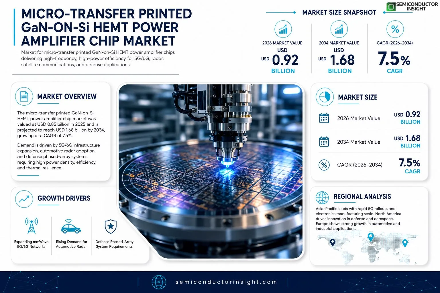
Micro‑transfer printed GaN‑on‑Si HEMT power amplifier chip market size was valued at USD 0.85 billion in 2025. The market is projected to grow from USD 0.92 billion in 2026 to USD 1.68 billion by 2034, exhibiting a CAGR of 7.5% during the forecast period.
Micro‑transfer printed GaN‑on‑Si HEMT (high‑electron‑mobility transistor) power amplifier chips combine gallium nitride epitaxy on silicon substrates with a precision transfer printing process that enables high‑frequency, high‑power density performance while reducing material costs and thermal resistance. This technology leverages the superior electron mobility of GaN and the mechanical robustness of Si, delivering efficient amplification for radar, satellite communications, and emerging 5G/6G infrastructure.The market is accelerating because telecom operators are expanding mmWave networks, automotive manufacturers demand compact high‑power solutions for electric vehicle radar, and defense sectors seek rugged components for phased‑array systems. Furthermore, recent collaborations between leading semiconductor foundries and equipment suppliers have streamlined the micro‑transfer workflow, shortening time‑to‑market and driving adoption across multiple verticals.
MARKET DRIVERS
Rising Demand in 5G Infrastructure
The rollout of 5G networks worldwide is creating a significant need for high‑frequency, high‑efficiency power amplifier chips. Micro‑transfer printed GaN‑on‑Si HEMT technology offers the linearity and power density required for millimeter‑wave base stations, making it a preferred solution for operators seeking to meet aggressive latency and bandwidth targets.
Efficiency Gains through Micro‑Transfer Printing
Micro‑transfer printing enables precise placement of GaN‑on‑Si HEMT dies, reducing parasitic losses and enhancing overall conversion efficiency. This process advantage aligns with the industry’s push for lower power consumption in data‑center interconnects and satellite communications.
➤ “Adoption of micro‑transfer printed GaN‑on‑Si HEMT amplifiers is projected to accelerate as OEMs prioritize thermal performance and size reduction.”
Furthermore, the compact form factor achieved through this technology supports emerging applications such as unmanned aerial vehicles and wearable radars, expanding the addressable market beyond traditional telecom equipment.
MARKET CHALLENGES
Manufacturing Yield Variability
The micro‑transfer process involves delicate handling of microscopic chips, which can lead to inconsistent yields across production runs. Variability poses a cost challenge for manufacturers aiming to maintain competitive pricing while ensuring reliability.
Other Challenges
Cost Sensitivity
Even though GaN‑on‑Si substrates are cheaper than sapphire or SiC, the additional steps required for micro‑transfer printing increase overall unit cost. Price‑sensitive segments such as consumer IoT devices may delay adoption until economies of scale are realized.
MARKET RESTRAINTS
High Capital Expenditure for Tooling
Establishing a dedicated micro‑transfer printing line demands substantial upfront investment in precision alignment equipment and clean‑room infrastructure. Companies without deep financial resources may find it prohibitive to scale production, limiting market penetration in the short term.
MARKET OPPORTUNITIES
Emerging Automotive Radar Applications
Automotive manufacturers are integrating high‑resolution radar systems for advanced driver‑assistance and autonomous driving functions. The combination of high power density and thermal resilience offered by micro‑transfer printed GaN‑on‑Si HEMT power amplifier chips positions them as a strategic component for next‑generation radar modules, opening a robust growth corridor.
Micro-transfer printed GaN-on-Si HEMT power amplifier chip Market Trends
Accelerated Adoption in Telecom mmWave Networks
The telecom sector is witnessing a swift expansion of millimeter‑wave infrastructure, and the micro‑transfer printed GaN‑on‑Si HEMT power amplifier chip is emerging as a preferred solution. By leveraging GaN’s high electron mobility on robust silicon platforms, these chips deliver the high‑frequency performance required for dense antenna arrays while maintaining lower thermal resistance, which aligns with the power‑density demands of modern 5G deployments and the anticipated 6G ecosystem. The precision transfer‑printing process shortens integration cycles, reduces material wastage, and enables designers to fabricate compact amplifier modules that fit within the limited space of base‑station hardware. As a result, network operators can upgrade antenna panels more rapidly, supporting both increased capacity and new spectrum bands with minimal disruption.
Other Trends
Automotive Radar Consolidation
Automotive manufacturers are increasing demand for compact, high‑power amplification to support radar sensors in electric vehicles and advanced driver‑assistance systems. The micro‑transfer printed approach reduces material costs and footprint, making it suitable for integration into front‑and‑rear radar modules that must operate reliably across a wide temperature range and under vibration. Collaborative projects between chip designers, silicon foundries, and vehicle OEMs have accelerated prototype validation, allowing automotive engineers to evaluate system‑level performance earlier in the development cycle. This synergy shortens time‑to‑market for next‑generation radar solutions and positions the technology for high‑volume production in the upcoming model years.
Defense and Aerospace System Integration
Defense and aerospace programs are adopting the technology to meet ruggedness and performance criteria for phased‑array radar, electronic‑warfare, and satellite‑communication payloads. The combination of GaN’s high‑power capability with silicon’s mechanical resilience provides a durable platform that tolerates harsh environmental stresses, including extreme temperatures and shock loads. Recent partnerships between leading semiconductor foundries and equipment suppliers have refined the micro‑transfer workflow, improving yield and shortening lead times for qualified parts. These improvements align with the procurement cycles of defense agencies, enabling faster fielding of upgraded radar suites and supporting the transition to higher‑frequency bands for secure communications.
COMPETITIVE LANDSCAPE
Key Industry Players
Micro‑transfer Printed GaN‑on‑Si HEMT Power Amplifier Chip Competitive Overview
The competitive arena is presently dominated by a handful of semiconductor giants that have leveraged their advanced epitaxy lines and high‑volume manufacturing capabilities to commercialize micro‑transfer printed GaN‑on‑Si HEMT power amplifier chips. Qorvo leads the market with a portfolio that spans automotive radar, 5G base‑stations, and defense phased‑array systems, benefitting from its deep RF heritage and recent strategic acquisitions. MACOM and Infineon follow closely, each offering differentiated process‑integration solutions that reduce thermal resistance while maintaining high‑frequency gain. ON Semiconductor (formerly Efficient Power) capitalizes on its cost‑effective silicon substrate approach, positioning itself as the primary supplier for mass‑market EV radar modules. These leaders command the majority of the projected USD 1.68 billion market by 2034, driving price‑performance trade‑offs and setting industry standards for reliability and scalability.Beyond the top tier, a vibrant cohort of specialist firms and emerging startups enriches the ecosystem with niche innovations. GaN Systems focuses on high‑power density designs for aerospace and satellite communications, while Texas Instruments and Analog Devices target mixed‑signal integration for telecom front‑ends. NXP Semiconductors and Skyworks Solutions exploit their system‑on‑chip expertise to embed GaN‑on‑Si HEMTs within compact modules for IoT and edge‑computing applications. Wolfspeed (Cree) and STMicroelectronics bring legacy SiC experience into the silicon‑based domain, emphasizing ruggedness for defense platforms. Smaller players such as MicroX Technologies, Sumitomo Electric, and a growing portfolio of university‑spun ventures contribute proprietary transfer‑printing tooling and niche process patents that enable faster time‑to‑market for custom radar and 6G prototypes.
List of Key GaN‑on‑Si HEMT Companies Profiled
- Qorvo
- MACOM
- Infineon Technologies
- ON Semiconductor (Efficient Power)
- GaN Systems
- Texas Instruments
- Analog Devices
- NXP Semiconductors
- Skyworks Solutions
- Wolfspeed (Cree)
- STMicroelectronics
- MicroX Technologies
- Sumitomo Electric
Segment Analysis:
| Segment Category | Sub-Segments | Key Insights |
| By Type |
|
Hybrid Integration is emerging as the preferred architectural approach because it balances high‑frequency performance with flexible chip‑level packaging.
|
| By Application |
|
5G/6G Infrastructure drives the most compelling use cases for micro‑transfer printed GaN‑on‑Si HEMT chips.
|
| By End User |
|
Telecom Operators are the leading end‑user segment, motivated by the need to densify networks and meet latency expectations.
|
| By Technology Trend |
|
Micro‑transfer Printing Advances are reshaping the design landscape for power amplifier chips.
|
| By Market Driver |
|
Expanding mmWave Networks act as the primary catalyst, fostering adoption across multiple verticals.
|
Regional Analysis: North America
North America
The expansion of 5G networks across North America is creating a substantial demand for high-performance power amplifiers. These chips are essential for enabling faster data speeds, lower latency, and increased network capacity, driving innovation in base stations and mobile devices.
The aerospace and defense sectors in North America utilize advanced power amplifiers for radar systems, communication equipment, and electronic warfare applications. The need for reliable and high-power solutions in these critical systems fuels demand for micro-transfer printed GaN-on-Si HEMT chips.
The automotive industry is increasingly incorporating advanced electronic systems, including radar and wireless communication modules, which rely on high-performance power amplifiers. The growing adoption of electric vehicles further enhances the demand for these chips.
The proliferation of the Industrial Internet of Things (IIoT) is driving demand for robust and reliable wireless communication solutions. Micro-transfer printed GaN-on-Si HEMT power amplifier chips play a crucial role in enabling long-range and high-bandwidth connectivity for industrial applications.
Europe
Europe exhibits a steady growth trajectory in Micro-transfer printed GaN-on-Si HEMT power amplifier chip Market. Strong government initiatives supporting technological advancement and a robust industrial base are key factors contributing to this expansion. The automotive sector in Europe, with its emphasis on connected and autonomous vehicles, presents a significant opportunity for these power amplifier chips. Additionally, the telecommunications infrastructure in Europe is undergoing continuous upgrades to support 5G deployment, further boosting demand. The region’s strong focus on energy efficiency also drives innovation in power amplifier technologies.
Asia-Pacific
Asia-Pacific is poised to be the fastest-growing market for micro-transfer printed GaN-on-Si HEMT power amplifier chips. The region’s rapid industrialization, expanding telecommunications infrastructure, and significant investments in electronics manufacturing are primary drivers. China, in particular, represents a massive market opportunity due to its large-scale 5G deployment and growing demand for advanced electronic devices. The robust electronics manufacturing ecosystem in countries like South Korea and Taiwan also contributes significantly to the growth of this market segment.
South America
South America presents a moderate growth opportunity for micro-transfer printed GaN-on-Si HEMT power amplifier chips. The expanding telecommunications infrastructure and increasing adoption of mobile technologies are driving demand in this region. The growing industrial sector, particularly in Brazil and Argentina, also contributes to the market’s potential. However, economic fluctuations and infrastructure development challenges can pose obstacles to growth.
Middle East & Africa
The Middle East & Africa region is an emerging market for micro-transfer printed GaN-on-Si HEMT power amplifier chips. Significant investments in telecommunications infrastructure, particularly in countries like Saudi Arabia and the United Arab Emirates, are driving demand for these power amplifier chips. The growing adoption of 5G and the expanding industrial sector further contribute to the market’s potential. However, the region’s relatively nascent electronics manufacturing base and geopolitical factors can present challenges.
Report Scope
This market research report provides a comprehensive analysis of the Micro-transfer printed GaN-on-Si HEMT power amplifier chip Market , covering the forecast period 2026–2034. It offers detailed insights into market dynamics, technological advancements, competitive landscape, and key trends shaping the industry.
Key focus areas of the report include:
- Market Overview: ✅ The report begins with an overview outlining its current market scenario, key growth indicators, and industry transformation drivers. It discusses macroeconomic factors, demand–supply balance, regulatory landscape, and the strategic role of semiconductors in powering advancements across industries such as automotive, telecommunications, consumer electronics, and industrial automation.
- ✅ Market Size & Forecast: Historical data and future projections for revenue, unit shipments, and market value across major regions and segments.
- ✅ Segmentation Analysis: Detailed breakdown by product type, technology, application, and end-user industry to identify high-growth segments and investment opportunities.
- ✅ Regional Insights: Insights into market performance across North America, Europe, Asia-Pacific, Latin America, and the Middle East & Africa, including country-level analysis where relevant.
- ✅ Competitive Landscape: Profiles of leading market participants, including their product offerings, R&D focus, manufacturing capacity, pricing strategies, and recent developments such as mergers, acquisitions, and partnerships.
- ✅ Technology Trends & Innovation: Assessment of emerging technologies, integration of AI/IoT, semiconductor design trends, fabrication techniques, and evolving industry standards.
- ✅ Market Drivers & Restraints: Evaluation of factors driving market growth along with challenges, supply chain constraints, regulatory issues, and market-entry barriers.
- ✅ Stakeholder Insights: Insights for component suppliers, OEMs, system integrators, investors, and policymakers regarding the evolving ecosystem and strategic opportunities.
Primary and secondary research methods are employed, including interviews with industry experts, data from verified sources, and real-time market intelligence to ensure the accuracy and reliability of the insights presented.
FREQUENTLY ASKED QUESTIONS:
What is the current market size of Micro-transfer printed GaN-on-Si HEMT power amplifier chip Market?
-> Micro-transfer printed GaN-on-Si HEMT power amplifier chip Market was valued at USD 0.85 billion in 2025 and is expected to reach USD 1.68 billion by 2034, representing a CAGR of 7.5% over the forecast period.
Which key companies operate in Micro-transfer printed GaN-on-Si HEMT power amplifier chip Market?
-> Key players include leading semiconductor manufacturers and foundries that produce GaN‑on‑Si HEMT technologies; specific company names were not detailed in the provided data.
What are the key growth drivers?
-> Key growth drivers include expanding mmWave telecommunications networks, rising demand for compact high‑power radar solutions in electric vehicles, and increased adoption by defense sectors for rugged phased‑array systems.
Which region dominates the market?
-> Regional dynamics indicate strong demand, with Asia‑Pacific showing rapid adoption due to telecom roll‑outs, while Europe remains a significant market for automotive and defense applications.
What are the emerging trends?
-> Emerging trends include integration of micro‑transfer printing workflows to shorten time‑to‑market, collaborations between semiconductor foundries and equipment suppliers, and the development of GaN‑on‑Si solutions for 5G/6G infrastructure.

Get Sample Report PDF for Exclusive Insights
Report Sample Includes
- Table of Contents
- List of Tables & Figures
- Charts, Research Methodology, and more...