
MARKET INSIGHTS
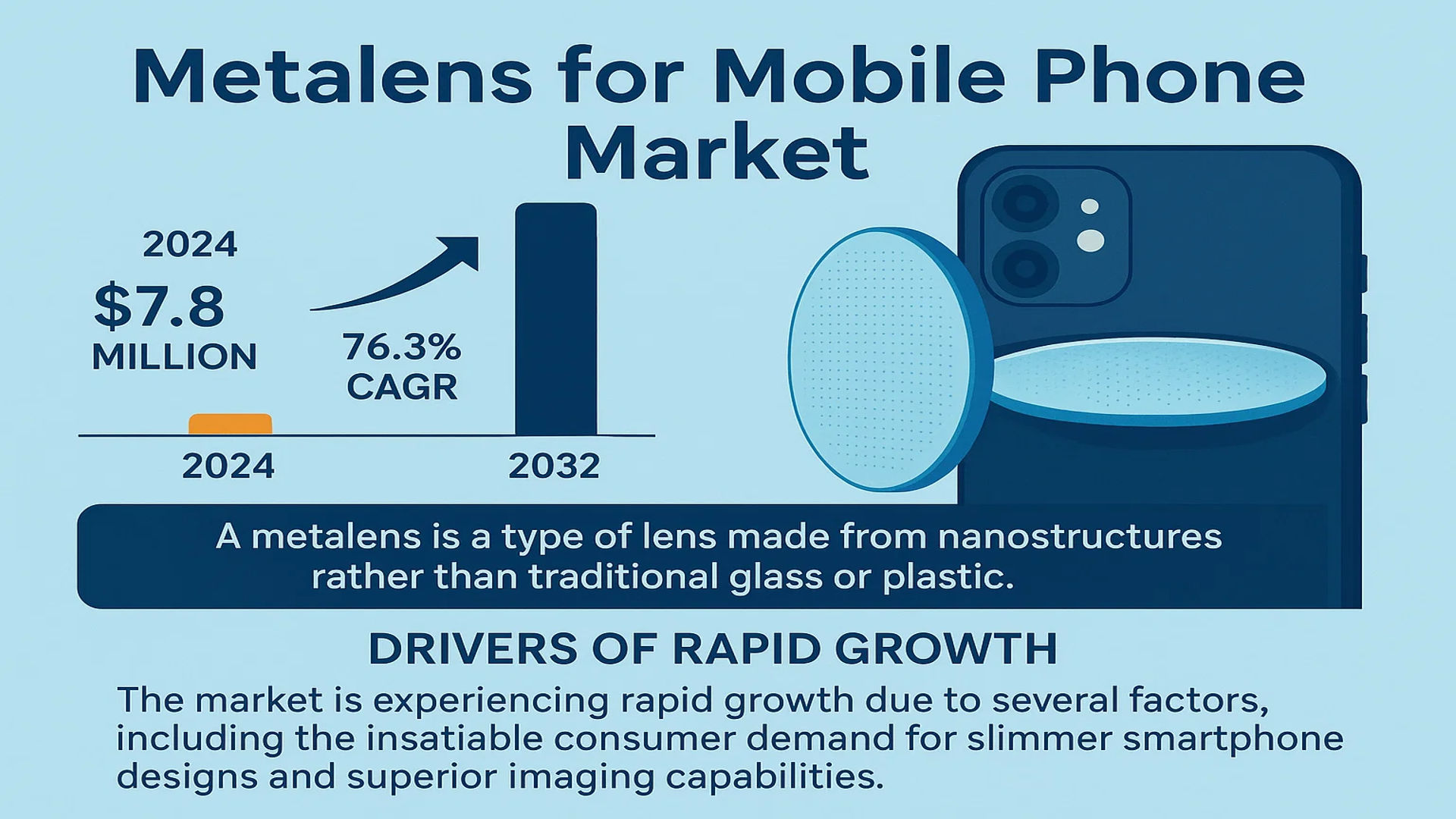
The global Metalens for Mobile Phone Market was valued at 7.8 million in 2024 and is projected to reach US$ 870 million by 2032, at a CAGR of 76.3% during the forecast period.
A metalens is a type of lens made from nanostructures rather than traditional glass or plastic. These nanostructures are designed to manipulate light at the nanoscale, allowing for the creation of lenses that are much thinner and lighter than traditional lenses. Metalenses have the potential to revolutionize a wide range of optical technologies, including cameras, microscopes, and virtual reality devices.
The market is experiencing rapid growth due to several factors, including the insatiable consumer demand for slimmer smartphone designs and superior imaging capabilities. Furthermore, advancements in nanotechnology and manufacturing processes are enabling the transition from customized prototypes to mass production. Key industry players are accelerating their strategic layouts; for instance, Metalenz, Inc. has secured significant funding and partnerships to commercialize its optical metasurface technology, signaling a major step towards widespread adoption in the mobile sector.
MARKET DYNAMICS
MARKET DRIVERS
Increasing Demand for Slimmer Smartphone Designs to Accelerate Metalens Adoption
The relentless pursuit of thinner and lighter smartphones represents a primary driver for metalens integration. Conventional multi-element glass lenses create significant camera bump protrusions, with some high-end models featuring camera modules over 10mm thick. Metalenses, being ultra-thin nanostructured surfaces typically under 1 micron in thickness, enable drastic reductions in the z-height of camera systems. This technological advantage allows OEMs to achieve sleeker form factors without compromising optical performance, addressing a critical consumer preference for elegant, pocketable devices. The ability to replace multiple traditional lens elements with a single metalens layer simplifies assembly and reduces the overall module footprint, making it highly attractive for space-constrained mobile applications.
Superior Optical Performance Characteristics to Drive Market Penetration
Metalenses offer exceptional optical capabilities that surpass traditional refractive optics in several key metrics. These nanostructured surfaces demonstrate remarkable light manipulation precision, achieving numerical apertures exceeding 0.8 while maintaining sub-wavelength thickness. Their unique phase modulation properties enable complete elimination of chromatic aberration, a persistent challenge in mobile photography. Additionally, metalenses provide enhanced focusing efficiency across visible and infrared spectra, with some demonstrations achieving focusing efficiencies exceeding 90% at specific wavelengths. This performance superiority translates to improved image quality, better low-light performance, and more accurate depth sensing—features increasingly demanded by consumers who use smartphone cameras as their primary imaging devices. The technology’s inherent capacity for advanced computational imaging applications further strengthens its value proposition for next-generation mobile photography.
Rising Investments in Advanced Manufacturing Capabilities to Fuel Commercialization
Substantial capital investments in semiconductor-compatible manufacturing processes are accelerating metalens commercialization. The technology leverages existing CMOS fabrication infrastructure, with production costs decreasing as foundries achieve higher throughput and yield rates. Recent advancements in nanoimprint lithography have demonstrated capability to produce metalenses at scale, with some processes achieving feature sizes below 100nm across 300mm wafers. This manufacturing scalability enables cost structures that become competitive with traditional optics at volume production, particularly for applications requiring complex optical functions. The alignment with established semiconductor manufacturing ecosystems reduces barriers to mass production and facilitates integration with smartphone image sensors, creating a compelling pathway for widespread adoption in mobile devices.
MARKET RESTRAINTS
High Manufacturing Complexity and Yield Challenges to Constrain Market Expansion
Despite promising manufacturing compatibility, metalens production faces significant technical hurdles that restrain market growth. The creation of high-efficiency metalenses requires extremely precise nanostructure patterning with feature sizes often below the diffraction limit. Current manufacturing processes struggle with defect densities that impact optical performance, particularly for larger aperture designs required in mobile applications. Yield rates for complex metalens structures remain below commercial viability thresholds, with some production lines reporting yields under 60% for designs requiring sub-100nm features. This manufacturing complexity translates to higher production costs compared to mature glass and plastic optics, creating economic barriers for price-sensitive mobile applications where component costs are constantly pressured downward.
Limited Field of View and Performance Trade-offs to Hinder Widespread Adoption
Metalens technology currently exhibits performance limitations that present substantial adoption barriers. The most significant constraint involves limited field of view capabilities, with most demonstrated metalenses achieving maximum fields below 20 degrees without additional optical elements. This restriction conflicts with mobile photography trends toward wider angles and multi-camera systems. Additionally, metalenses demonstrate pronounced efficiency variations across the visible spectrum, with performance typically optimized for specific wavelengths rather than providing uniform response across all colors. These technical compromises necessitate hybrid approaches combining metalenses with traditional optics, thereby reducing the technology’s space-saving advantages and increasing system complexity. Such performance trade-offs create implementation challenges for smartphone manufacturers who must deliver consistent imaging quality across diverse shooting scenarios.
Intellectual Property Barriers and Standardization Gaps to Slow Market Development
The metalens landscape is characterized by fragmented intellectual property ownership and insufficient standardization, creating implementation barriers. Numerous patents cover fundamental metalens designs and manufacturing methods, leading to potential licensing complications for smartphone manufacturers. This IP complexity increases development risks and may result in protracted negotiations that delay product integration timelines. Furthermore, the absence of established industry standards for metalens specifications, testing methodologies, and performance metrics creates uncertainty regarding quality assurance and interoperability. Without clear standards, smartphone manufacturers face challenges in evaluating and comparing metalens solutions from different suppliers, potentially slowing adoption decisions and investment commitments in this emerging technology.
MARKET CHALLENGES
Material Durability and Environmental Stability Concerns Pose Significant Challenges
Metalens structures face substantial durability challenges that impact their suitability for mobile applications. The nanometer-scale features essential for optical performance are particularly vulnerable to environmental factors including humidity, temperature fluctuations, and mechanical stress. Testing has revealed that certain metalens materials exhibit degradation under typical smartphone usage conditions, with some designs showing performance reduction after exposure to elevated temperatures commonly reached during extended camera use. Additionally, the structural integrity of these delicate nanostructures presents concerns regarding shock resistance and scratch protection—critical factors for devices subjected to daily handling and potential impacts. These durability issues necessitate protective measures that may compromise the technology’s thickness advantages or increase manufacturing complexity.
Other Challenges
Supply Chain Maturity
The metalens supply chain remains underdeveloped compared to traditional optics, creating reliability concerns for high-volume smartphone production. Limited availability of production-grade fabrication capacity, coupled with immature quality control processes, presents risks for manufacturers requiring consistent component supplies for mass-market devices. The specialized equipment and expertise required for metalens production further constrain rapid scaling of manufacturing capabilities to meet potential smartphone industry demand.
Integration Complexity
Successfully integrating metalenses into existing smartphone camera architectures presents substantial engineering challenges. The technology requires rethinking of optical design principles, sensor compatibility, and image processing algorithms. This integration complexity demands significant R&D investment and cross-disciplinary expertise that many smartphone manufacturers may lack, potentially delaying adoption timelines and increasing development costs for early implementations.
MARKET OPPORTUNITIES
Emerging Applications in 3D Sensing and Computational Photography to Create New Growth Avenues
Metalens technology enables breakthrough capabilities in advanced mobile imaging applications beyond conventional photography. Their unique light manipulation properties make them ideally suited for structured light and time-of-flight 3D sensing systems, potentially enhancing facial recognition accuracy and augmented reality experiences. The technology’s capacity for creating complex phase profiles supports advanced computational photography techniques including light field capture and single-shot depth mapping. These capabilities align perfectly with smartphone industry trends toward more sophisticated imaging systems that support emerging applications in computational photography, augmented reality, and machine vision. The integration of metalenses could enable new user experiences and functionality differentiators that drive premium smartphone segmentation and create additional value for consumers.
Advancements in Multi-functional Metalens Designs to Unlock Integration Opportunities
Recent research breakthroughs in multi-functional metalens configurations present significant opportunities for market expansion. Developments in metasurface technology now enable single metalens layers to perform multiple optical functions simultaneously, such as combining imaging, beam steering, and spectral filtering capabilities. This multifunctionality could dramatically reduce the number of separate optical components required in smartphone cameras, further minimizing module size while enhancing system performance. The ability to create metalenses with dynamically tunable properties through integration with electro-optic materials opens possibilities for adaptive optics in mobile devices. These advancements could enable new camera features including variable focus without moving parts, real-time optical image stabilization, and programmable spectral response—capabilities that would represent significant competitive advantages for adopting manufacturers.
Growing Ecosystem Partnerships and Technology Licensing to Accelerate Commercialization
The metalens market is witnessing increasing strategic collaborations between technology developers, semiconductor foundries, and smartphone manufacturers that create substantial growth opportunities. These partnerships facilitate technology transfer, manufacturing scale-up, and integration expertise development essential for successful commercialization. Several leading metalens technology companies have established manufacturing partnerships with major semiconductor foundries, leveraging existing high-volume production capabilities to address scale and cost challenges. Additionally, licensing agreements with smartphone manufacturers provide revenue streams for technology developers while reducing R&D risks for device makers. This collaborative ecosystem approach accelerates technology maturation and creates pathways for rapid adoption once performance and cost targets are achieved, potentially leading to accelerated market penetration in the mobile sector.
METALENS FOR MOBILE PHONE MARKET TRENDS
Advancements in Nanofabrication and Miniaturization Drive Market Evolution
The metalens market for mobile phones is experiencing a transformative phase, primarily driven by significant advancements in nanofabrication techniques and the relentless pursuit of device miniaturization. These flat optics, composed of subwavelength nanostructures, manipulate light with unprecedented precision, enabling smartphone manufacturers to overcome the physical limitations of traditional curved glass lenses. The primary catalyst for this trend is the industry-wide shift towards slimmer form factors without compromising optical performance. While the technology was once confined to research laboratories, breakthroughs in semiconductor manufacturing processes, particularly deep ultraviolet (DUV) and extreme ultraviolet (EUV) lithography, have enabled mass production at commercially viable scales. This manufacturing evolution is critical because metalenses require feature sizes below 100 nanometers, pushing the boundaries of current production capabilities. Furthermore, the integration of computational imaging algorithms with metalens designs has created synergistic effects, enhancing image quality beyond what either technology could achieve independently. This convergence of nanotechnology and artificial intelligence is setting new benchmarks for mobile photography, with several prototype devices already demonstrating superior low-light performance and reduced chromatic aberration compared to conventional multi-lens systems.
Other Trends
Enhanced Imaging Capabilities and Multi-Spectral Sensing
The integration of multi-spectral sensing capabilities represents a significant trend driving metalens adoption in mobile devices. Modern smartphones are evolving beyond traditional photography into comprehensive sensing platforms, requiring optics that can handle diverse wavelengths from visible to infrared spectra. Metalenses offer unique advantages here because their nanostructures can be engineered to simultaneously focus multiple wavelengths without the need for complex lens assemblies. This capability is particularly valuable for emerging applications such as 3D facial recognition, augmented reality overlays, and computational photography features like portrait mode and night mode. The ability to create multi-functional optical surfaces that replace several conventional lens elements directly addresses the space constraints in mobile devices while adding sophisticated features. Manufacturers are particularly interested in metalenses that can operate across both visible and near-infrared spectra, enabling advanced biometric authentication and environmental sensing. This trend is accelerating as consumer expectations for mobile photography continue to rise, with demand for professional-grade imaging capabilities in pocket-sized devices becoming increasingly standard across all market segments.
Supply Chain Integration and Manufacturing Scalability
The maturation of metalens manufacturing processes and their integration into existing mobile device supply chains constitutes a crucial market trend. While initial production was characterized by high costs and low yields, recent developments in nanoimprint lithography and other replication techniques have dramatically improved production efficiency. The market is witnessing a shift from customized, small-batch production toward standardized manufacturing processes that can support volume production requirements of mobile phone manufacturers. This scalability is essential for meeting the anticipated demand, particularly as industry projections suggest that over 25% of premium smartphones will incorporate metalens technology within the next three years. The manufacturing ecosystem is also evolving, with traditional optical component suppliers transitioning their expertise toward metasurface production while new specialized entrants focus exclusively on metalens development. This dual-track approach is accelerating technology adoption while ensuring that manufacturing quality and consistency meet the rigorous standards required for consumer electronics. Furthermore, the compatibility of metalens fabrication with existing semiconductor manufacturing infrastructure provides a significant advantage, allowing for rapid scaling using proven production methodologies rather than requiring entirely new manufacturing paradigms.
COMPETITIVE LANDSCAPE
Key Industry Players
Companies Accelerate R&D and Strategic Partnerships to Capture Emerging Market Opportunities
The global metalens for mobile phone market exhibits a dynamic and evolving competitive structure, characterized by a mix of specialized startups, established optics firms, and technology developers racing to commercialize this transformative technology. While the market is still nascent, its projected growth to $870 million by 2032 has spurred intense activity and strategic positioning. The landscape is currently fragmented but shows signs of consolidation as larger entities begin to acquire promising technologies and form critical partnerships with smartphone OEMs.
Metalenz, Inc., a spin-out from Harvard University, is widely recognized as a pioneering force. The company’s leadership is attributed to its foundational IP portfolio covering optical metasurfaces and its successful Series B funding round, which positions it for high-volume manufacturing scaling. Their collaboration with STMicroelectronics in 2023 to co-develop metasurface optics for consumer devices marks a significant step toward mass production, solidifying their position as a key technology enabler for major smartphone brands.
Similarly, Radiant Opto-Electronics Corporation (operating through its NIL Technology division) holds a significant technological and manufacturing advantage. The company leverages its deep expertise in nanoimprint lithography (NIL), a critical fabrication technique for metasurfaces. This capability allows them to address one of the industry’s primary challenges: moving from lab-scale prototypes to cost-effective, high-yield mass production. Their established presence in Asia, a hub for consumer electronics manufacturing, provides a substantial strategic edge.
These front-runners are not operating in a vacuum. Other agile players are making notable strides. MetaLenX is focusing on advanced design software and simulation tools tailored for metalens development, which are crucial for reducing design iteration times. Meanwhile, Chinese firms like Hangzhou Najing Technology and SHPHOTONICS are strengthening their market presence through significant investments in domestic R&D and pursuing partnerships with local smartphone manufacturers. This is particularly relevant given that Asia is anticipated to be the largest and fastest-adopting regional market.
Furthermore, these companies’ growth is fueled by continuous innovation in material science and fabrication processes. Advancements in using high-index transparent materials and mastering etching techniques for creating precise nanostructures are directly improving optical efficiency and production viability. The competitive intensity is therefore not just about market share but also about achieving technological milestones that lower costs and improve performance, thereby unlocking broader adoption across mid-range and eventually entry-level smartphone segments.
List of Key Metalens for Mobile Phone Companies Profiled
- Metalenz, Inc. (U.S.)
- Radiant Opto-Electronics (NIL Technology) (Denmark)
- MetaLenX (South Korea)
- Hangzhou Najing Technology (China)
- SHPHOTONICS (China)
Segment Analysis:
By Type
Visible Light Metalens Segment Leads Due to Critical Role in Main Camera Systems
The market is segmented based on type into:
- Visible Light Metalens
- Infrared Metalens
By Application
Android Phone Segment Dominates Owing to High Market Share and Manufacturer Adoption
The market is segmented based on application into:
- Android Phone
- IOS Phone
- Hongmeng Phone
- Other
By Function
Imaging Function Holds Largest Share Driven by Consumer Demand for Superior Camera Performance
The market is segmented based on function into:
- Imaging
- Sensing
- 3D Depth Mapping
- Augmented Reality
By Manufacturing Technology
Nanoimprint Lithography Gains Traction for Cost-Effective Mass Production
The market is segmented based on manufacturing technology into:
- Electron-Beam Lithography
- Nanoimprint Lithography
- Photolithography
- Focused Ion Beam Milling
Regional Analysis: Metalens for Mobile Phone Market
Asia-Pacific
The Asia-Pacific region is the dominant force and primary growth engine for the metalens market in mobile phones, driven by its unparalleled concentration of smartphone manufacturing and R&D. China, South Korea, and Japan collectively house the world’s leading smartphone OEMs—including Samsung, Xiaomi, OPPO, and Vivo—and their extensive supply chains. This ecosystem fosters rapid adoption of cutting-edge components like metalenses, which are critical for achieving slimmer form factors and superior camera performance, key differentiators in this highly competitive market. The region’s significant investment in semiconductor and nanotechnology research, supported by government initiatives, accelerates the transition from R&D to mass production. While cost sensitivity remains a factor for mid-range devices, the demand for premium features in flagship models from these manufacturers positions Asia-Pacific at the forefront of metalens integration, making it the largest and most advanced market globally.
North America
North America, particularly the United States, is a hub for technological innovation and early-stage investment in metamaterial and nanophotonics research. The region’s strength lies in its robust venture capital landscape and the presence of pioneering companies like Metalenz, Inc., which are developing foundational IP for metalens technology. High consumer demand for premium mobile devices with advanced imaging capabilities, such as those from Apple and Google, creates a strong pull for innovative optical solutions. However, the market’s progression is tempered by the region’s limited large-scale manufacturing capacity for consumer electronics. Most actual integration into handsets occurs through partnerships with Asian manufacturing partners. Consequently, North America’s role is predominantly as an innovation and design center, driving the technological roadmap that will eventually be mass-produced elsewhere.
Europe
Europe exhibits a strong research-oriented market characterized by significant academic and institutional advancements in photonics, supported by framework programs like Horizon Europe. Countries such as Germany, the UK, and the Benelux region host specialized firms and research institutes pushing the boundaries of metasurface design and applications. The market is driven by a focus on high-value engineering, precision manufacturing, and quality, aligning with the performance requirements of metalenses. However, similar to North America, Europe’s consumer electronics manufacturing base is relatively limited. Adoption is therefore expected to be slower and more focused on high-end niche applications and partnerships with global smartphone brands rather than volume production. Strict regulations on materials and electronic waste also influence design parameters, encouraging sustainable innovation in new component technologies.
South America
The metalens market in South America is in a nascent stage, primarily due to economic constraints and a smartphone market focused on value and mid-range devices rather than cutting-edge technology adoption. Countries like Brazil and Argentina have large consumer bases, but local manufacturing is often limited to assembly operations, with key components imported. The high cost associated with nascent technologies like metalenses presents a significant barrier to widespread adoption in the short term. Market growth is contingent on global price reductions in metalens manufacturing and the trickle-down of technology into more affordable phone segments. While long-term potential exists as the technology matures, current market activity is minimal, with growth largely dependent on the strategies of multinational smartphone companies operating in the region.
Middle East & Africa
The Middle East & Africa region represents an emerging market with potential for long-term growth, though it is not currently a significant driver for metalens adoption. Wealthier nations in the Gulf Cooperation Council (GCC), such as the UAE and Saudi Arabia, have high smartphone penetration rates and a consumer appetite for luxury and flagship devices. This could create a niche market for phones incorporating advanced technologies like metalenses. However, the region overall lacks local manufacturing or R&D infrastructure for such components. Adoption is entirely dependent on imports and the global product strategies of major brands. Economic disparities and a focus on more affordable mobile solutions across much of Africa further limit near-term opportunities, making this a region to watch for future growth as the technology becomes more mainstream and cost-effective.
Report Scope
This market research report provides a comprehensive analysis of the global and regional Metalens for Mobile Phone markets, covering the forecast period 2025–2032. It offers detailed insights into market dynamics, technological advancements, competitive landscape, and key trends shaping the industry.
Key focus areas of the report include:
- Market Size & Forecast: Historical data and future projections for revenue, unit shipments, and market value across major regions and segments.
- Segmentation Analysis: Detailed breakdown by product type, technology, application, and end-user industry to identify high-growth segments and investment opportunities.
- Regional Outlook: Insights into market performance across North America, Europe, Asia-Pacific, Latin America, and the Middle East & Africa, including country-level analysis where relevant.
- Competitive Landscape: Profiles of leading market participants, including their product offerings, R&D focus, manufacturing capacity, pricing strategies, and recent developments such as mergers, acquisitions, and partnerships.
- Technology Trends & Innovation: Assessment of emerging technologies, integration of AI/IoT, semiconductor design trends, fabrication techniques, and evolving industry standards.
- Market Drivers & Restraints: Evaluation of factors driving market growth along with challenges, supply chain constraints, regulatory issues, and market-entry barriers.
- Stakeholder Analysis: Insights for component suppliers, OEMs, system integrators, investors, and policymakers regarding the evolving ecosystem and strategic opportunities.
Primary and secondary research methods are employed, including interviews with industry experts, data from verified sources, and real-time market intelligence to ensure the accuracy and reliability of the insights presented.
FREQUENTLY ASKED QUESTIONS:
What is the current market size of Global Metalens for Mobile Phone Market?
-> Metalens for Mobile Phone Market was valued at 7.8 million in 2024 and is projected to reach US$ 870 million by 2032, at a CAGR of 76.3% during the forecast period.
Which key companies operate in Global Metalens for Mobile Phone Market?
-> Key players include Metalenz, Inc., Radiant Opto-Electronics (NIL Technology), MetaLenX, Hangzhou Najing Technology, and SHPHOTONICS, among others.
What are the key growth drivers?
-> Key growth drivers include demand for thinner smartphone designs, superior optical performance requirements, and advancements in nanotechnology manufacturing.
Which region dominates the market?
-> Asia-Pacific is the dominant market, driven by manufacturing hubs in China and Japan, while North America leads in technological innovation and R&D.
What are the emerging trends?
-> Emerging trends include integration with AI-powered camera systems, multi-spectral imaging capabilities, and sustainable nanofabrication processes.

Get Sample Report PDF for Exclusive Insights
Report Sample Includes
- Table of Contents
- List of Tables & Figures
- Charts, Research Methodology, and more...
 Download Sample Report PDF

