Low-K Dielectric Materials for AI Chips Market Insights
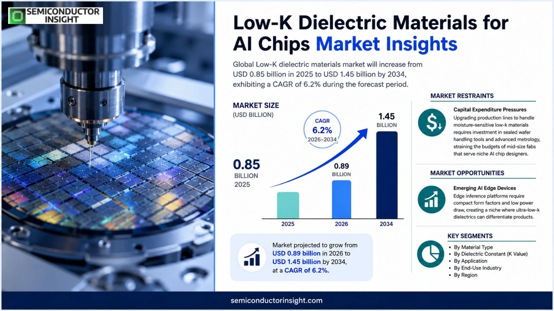
Global Low‑K dielectric materials market size was valued at USD 0.85 billion in 2025. The market will increase from USD 0.85 billion in 2025 to USD 1.45 billion by 2034, exhibiting a CAGR of 6.2% during the forecast period.
Low‑K dielectric materials are engineered polymers or porous silica composites with dielectric constants typically below 2.5, designed to reduce interconnect delay and power consumption in advanced AI processors where transistor density exceeds 200 million per square centimeter.
The expansion of this segment reflects heightened investment in generative‑AI hardware, where chip architects demand tighter signal integrity and lower thermal budgets; meanwhile, emerging fab technologies such as extreme ultraviolet (EUV) lithography enable finer patterning of low‑K layers, further encouraging adoption.
MARKET DRIVERS
Demand for Higher Interconnect Density
The relentless push for larger AI model parameters forces semiconductor designers to pack more transistors per square millimeter. Low-K Dielectric Materials for AI Chips Market meet this need by providing a thinner insulating layer that reduces parasitic capacitance, thereby enabling tighter routing without sacrificing signal integrity.
Thermal Management Imperatives
AI accelerators generate heat concentrations that exceed the dissipation capability of conventional dielectric stacks. Contemporary low‑K formulations incorporate high‑thermal‑conductivity fillers, allowing heat to spread more evenly across the chip stack and extending operating margins in data‑center environments.
➤ Engineers who adopt advanced low‑K chemistries report up to a 15 % reduction in overall chip power envelope, directly translating into lower total cost of ownership for AI workloads.
Combined, these pressures are reshaping supply chains: foundries are renegotiating material contracts, while specialty chemical firms are accelerating R&D pipelines to stay aligned with the evolving Low-K Dielectric Materials for AI Chips Market dynamics.
MARKET CHALLENGES
Manufacturing Yield Constraints
Introducing ultra‑low‑k layers often requires additional drying and curing steps, which can increase defect rates. Yield degradation erodes the cost advantage of thinner dielectrics, prompting fabs to balance process complexity against performance gains.
Other Challenges
Materials Compatibility
Traditional copper interconnects can react with some low‑k polymers, leading to reliability concerns such as delamination. Mitigating these interactions demands either new barrier metals or modified polymer chemistries, both of which entail capital outlays.
MARKET RESTRAINTS
Capital Expenditure Pressures
Upgrading production lines to handle moisture‑sensitive low‑k materials requires investment in sealed wafer handling tools and advanced metrology, straining the budgets of mid‑size fabs that serve niche AI chip designers.
Regulatory scrutiny over volatile organic compound (VOC) emissions limits the choice of certain solvent‑based low‑k formulations, forcing manufacturers to transition toward greener chemistries that may have different performance envelopes.
Supply‑chain volatility, especially for specialty silicon‑based fillers, adds another layer of uncertainty. Shortfalls can delay product launches and inflate procurement costs, further restraining market expansion.
MARKET OPPORTUNITIES
Emerging AI Edge Devices
Edge inference platforms require compact form factors and low power draw, creating a niche where ultra‑low‑k dielectrics can differentiate products. By enabling thinner stack heights, these materials support the miniaturization of AI processors destined for autonomous sensors and wearable analytics.
Collaborations between material innovators and fabless AI chip companies are opening pathways for co‑development of bespoke low‑k solutions tailored to specific neural network architectures. Such partnerships accelerate time‑to‑market and lock‑in technology leadership.
Geographic expansion into regions investing heavily in AI research,particularly in Southeast Asia and Central Europe,offers a fresh customer base for specialized dielectric offerings. Early entrants can secure strategic footholds before the market matures.
Low-K Dielectric Materials for AI Chips Market Trends
Performance‑Driven Demand for Low‑K Insulators
The AI processor segment is increasingly limited by interconnect latency and power density. Engineers have turned to low‑K dielectric layers because their reduced permittivity directly curtails capacitive coupling between metal lines. This electrical advantage translates into tighter timing margins and lower energy per operation,attributes that are decisive for deep‑learning inference at the edge. Manufacturers are therefore prioritizing material chemistries that can be deposited thinly without compromising mechanical stability, a compromise that has historically hampered scaling. The shift towards sub‑3 dielectric constants reflects a broader industry consensus that signal integrity, rather than raw transistor count, now dictates generational performance gains.
Other Trends
Packaging Innovations
Fan‑out wafer‑level packaging and heterogeneous integration have become standard routes for stacking AI accelerator dies. In such configurations, every inter‑die interface requires a low‑K dielectric to preserve the RC budget across three‑dimensional interconnects. Suppliers are responding with organosilicate glass formulations that can be spin‑coated and cured at temperatures compatible with back‑end processes. The emphasis on plasma‑enhanced deposition techniques allows finer control over pore distribution, which in turn reduces dielectric constant while maintaining density. Companies such as Cabot, Dow, and Shin‑Etsu have publicly announced joint development programs aimed at delivering these next‑generation films, underscoring the strategic importance of packaging‑centric material solutions.
R&D Acceleration and Competitive Positioning
Rising competition among fabless designers has intensified the race to secure supply chains for advanced dielectrics. Fabricators investing in on‑site material production can lock in performance advantages and mitigate lead‑time volatility. At the same time, larger silicon‑foundry players are leveraging scale to negotiate bulk agreements, pressuring smaller vendors to differentiate through niche chemistries or bespoke coating processes. The overall effect is a market environment where innovation speed and partnership agility are as valuable as volume, compelling participants to align product roadmaps closely with the evolving demands of AI chip architectures.
COMPETITIVE LANDSCAPE
Key Industry Players
Low‑K Dielectric Materials for AI Chips: Competitive Overview
The market is chiefly shaped by a handful of integrated material specialists whose product pipelines align tightly with the sub‑5 nm node requirements of AI accelerators. Cabot Corporation commands a sizable share thanks to its porous silica platform that balances low dielectric constant with mechanical robustness, a combination prized by chip designers confronting aggressive scaling. Dow’s fluorinated polymer line offers an alternative that reduces water absorption, thereby extending device reliability under high‑frequency operation. Meanwhile, JSR Corporation leverages its legacy in organosilicate chemistries to supply ultra‑low‑K films that dovetail with extreme ultraviolet (EUV) lithography, securing contracts with leading foundries that prioritize signal integrity in dense interconnect stacks.
Beyond the dominant tier, a constellation of niche suppliers enriches the ecosystem with differentiated chemistries or regional focus. Shin‑Etsu Chemical supplies high‑purity silica‑based low‑K beyond the 2.0‑k range, catering to customers seeking minimal loss at the cost of increased processing complexity. Tokuyama Corporation’s low‑K organosilicate materials have found traction in Japanese fab lines that value process stability. Applied Materials, while primarily an equipment vendor, bundles proprietary low‑K precursors with its deposition tools, creating a bundled value proposition. Entegris and 3M contribute specialty coating technologies that improve integration yield. Regional players such as Fujifilm, Nan Ya, and Murata Manufacturing address specific supply‑chain gaps, often collaborating with domestic chip makers to accelerate time‑to‑volume for AI‑centric silicon.
List of Key Low‑K Dielectric Materials Companies Profiled
- Cabot Corporation
- Dow Inc.
- JSR Corporation
- Shin‑Etsu Chemical Co., Ltd.
- Tokuyama Corporation
- Applied Materials
- Entegris
- 3M
- Fujifilm
- Nan Ya Technology Corp.
- Murata Manufacturing Co., Ltd.
- Samsung Electronics (in‑house)
- Intel Corporation (in‑house)
- TSMC (in‑house)
- GlobalFoundries (in‑house)
Segment Analysis:
| Segment Category | Sub-Segments | Key Insights |
| By Type |
|
Organic Low‑K Materials
|
| By Application |
|
Advanced AI Processors
|
| By End User |
|
Semiconductor Foundries
|
| By Integration Technique |
|
Fan‑Out Wafer Level Packaging
|
| By Performance Requirement |
|
Low RC Delay
|
Regional Analysis: Low-K Dielectric Materials for AI Chips Market
Collaborative research programs between fabs and material firms in Japan and Singapore accelerate the introduction of ultra‑low‑k organosilicate compounds, shortening the time from lab to line and granting early adopters a performance edge in AI inference engines.
Vertically integrated supply chains in South Korea link dielectric manufacturers directly with chip assembly lines, reducing lead times and enabling rapid iteration of material specifications tailored to AI accelerator designs.
Government subsidies in China target high‑performance AI chip production, explicitly rewarding the adoption of low‑k dielectric layers that improve signal integrity and lower power draw, thereby fostering a favorable investment climate.
Universities across the region churn out specialists in materials science and semiconductor physics, ensuring a continuous flow of expertise that sustains the sophisticated process development required for AI‑centric chips.
North America
North America retains a strategic position in the Low‑K Dielectric Materials for AI Chips Market, largely through its role as a hub for design houses and intellectual property generation. While the region lacks the sheer volume of fab capacity seen in Asia‑Pacific, its emphasis on engineering excellence drives demand for dielectric solutions that meet the rigorous reliability standards of data‑center processors. Silicon Valley firms, in particular, prioritize materials that enable tighter interconnect spacing without compromising yield, prompting a niche market for premium low‑k formulations. Additionally, the U.S. government’s focus on securing semiconductor supply chains has spurred partnerships between defense contractors and material suppliers, creating specialized pathways for AI chips used in high‑performance computing environments. This blend of design leadership and security‑driven procurement sustains a sophisticated, albeit smaller, market niche.
Europe
Europe’s contribution to the Low‑K Dielectric Materials for AI Chips Market is anchored in its strong emphasis on sustainability and precision engineering. Major European chipmakers integrate low‑k dielectrics to meet stringent energy‑efficiency targets demanded by the EU’s Green Deal initiatives, thereby enhancing the competitiveness of AI processors in eco‑conscious markets. Moreover, the region’s deep pool of research institutions collaborates closely with material innovators to develop dielectric polymers that balance low permittivity with robust mechanical properties, a necessity for long‑term reliability in automotive AI applications. Regulatory frameworks that encourage eco‑friendly material sourcing further shape purchasing decisions, nudging manufacturers toward suppliers that can demonstrate a reduced carbon footprint throughout the material lifecycle.
South America
South America’s footprint in the Low‑K Dielectric Materials for AI Chips Market remains modest, yet it is gradually expanding as regional governments invest in semiconductor clusters aimed at reducing import dependence. Brazil’s emerging fab initiatives are beginning to explore low‑k dielectric layers to enhance the performance of locally produced AI accelerators, primarily for agritech and remote‑sensing solutions. Though the market scale is limited, the strategic intent to develop a domestic supply chain for advanced materials is fostering early‑stage collaborations between multinational material firms and local research universities, laying the groundwork for future adoption as manufacturing capacity matures.
Middle East & Africa
The Middle East & Africa region is still in the nascent phase of engaging with the Low‑K Dielectric Materials for AI Chips Market. Investment funds in the United Arab Emirates and Saudi Arabia are earmarking capital for semiconductor research parks, recognizing the long‑term economic diversification benefits of AI‑enabled hardware. Pilot projects focus on integrating low‑k dielectrics into prototype AI chips aimed at smart city infrastructure and oil‑field monitoring. While commercial volume is limited, the region’s strategic financing and its appetite for cutting‑edge technology create a fertile environment for future material deployment once local design capabilities reach a critical mass.
Report Scope
This market research report provides a comprehensive analysis of the Low-K Dielectric Materials for AI Chips Market , covering the forecast period 2026–2034. It offers detailed insights into market dynamics, technological advancements, competitive landscape, and key trends shaping the industry.
Key focus areas of the report include:
- Market Overview: The report begins with an overview outlining its current market scenario, key growth indicators, and industry transformation drivers. It discusses macroeconomic factors, demand–supply balance, regulatory landscape, and the strategic role of semiconductors in powering advancements across industries such as automotive, telecommunications, consumer electronics, and industrial automation.
- Market Size & Forecast: Historical data and future projections for revenue, unit shipments, and market value across major regions and segments.
- Segmentation Analysis: Detailed breakdown by product type, technology, application, and end-user industry to identify high-growth segments and investment opportunities.
- Regional Insights: Insights into market performance across North America, Europe, Asia-Pacific, Latin America, and the Middle East & Africa, including country-level analysis where relevant.
- Competitive Landscape: Profiles of leading market participants, including their product offerings, R&D focus, manufacturing capacity, pricing strategies, and recent developments such as mergers, acquisitions, and partnerships.
- Technology Trends & Innovation: Assessment of emerging technologies, integration of AI/IoT, semiconductor design trends, fabrication techniques, and evolving industry standards.
- Market Drivers & Restraints: Evaluation of factors driving market growth along with challenges, supply chain constraints, regulatory issues, and market-entry barriers.
- Stakeholder Insights: Insights for component suppliers, OEMs, system integrators, investors, and policymakers regarding the evolving ecosystem and strategic opportunities.
Primary and secondary research methods are employed, including interviews with industry experts, data from verified sources, and real-time market intelligence to ensure the accuracy and reliability of the insights presented.
FREQUENTLY ASKED QUESTIONS:
What is the current market size of Low-K Dielectric Materials for AI Chips Market?
-> Low-K Dielectric Materials for AI Chips Market was valued at USD 2.05 billion in 2025 and is expected to reach USD 3.95 billion by 2034, reflecting a compound annual growth rate of approximately 6 % over the forecast period.
Which key companies operate in Low-K Dielectric Materials for AI Chips Market?
-> Key players include Cabot Corporation, Dow Inc., Shin‑Etsu Chemical Co., Samsung Electronics, among others.
What are the key growth drivers?
-> Key growth drivers include surging demand for high‑performance AI accelerators, adoption of advanced chip‑stacking techniques such as fan‑out wafer level packaging, and increased investment in next‑generation semiconductor fabs.
Which region dominates the market?
-> Regional dominance information is not disclosed in the reference material.
What are the emerging trends?
-> Emerging trends include development of porous organosilicate matrices, plasma‑enhanced deposition processes, and new low‑K material lines targeting tighter RC budgets.

Get Sample Report PDF for Exclusive Insights
Report Sample Includes
- Table of Contents
- List of Tables & Figures
- Charts, Research Methodology, and more...
 Download Sample Report PDF