Japan AI Ceramic Electrostatic Chuck Surface Charge Uniformity Control Chip Market Insights
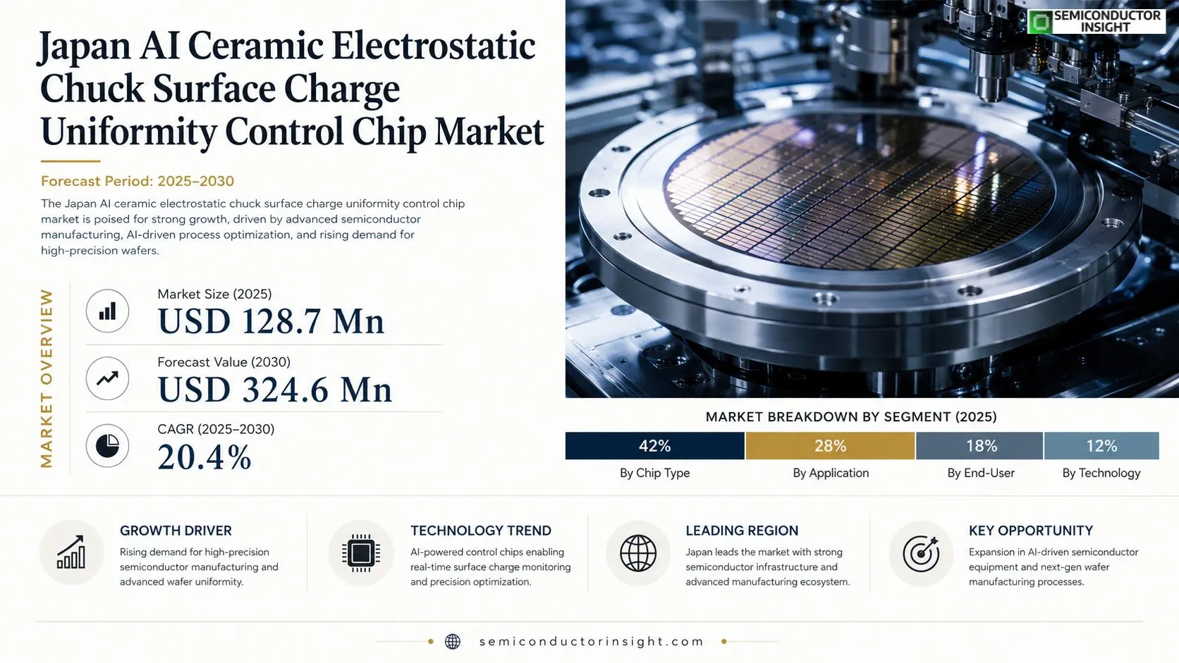
Japan AI ceramic electrostatic chuck surface charge uniformity control chip market size was valued at USD 112 million in 2025. The market is projected to grow from USD 118 million in 2025 to USD 215 million by 2034, exhibiting a CAGR of 7.0% during the forecast period.
The control chip integrates a silicon‑based AI processor with a high‑dielectric ceramic substrate to monitor and adjust charge distribution across the electrostatic chuck in real time. By leveraging machine‑learning algorithms, the chip predicts charge drift and modulates voltage bias, ensuring uniform wafer adhesion and reducing defect rates during semiconductor fabrication.The market is experiencing rapid expansion because semiconductor manufacturers are intensifying demand for higher yield and finer patterning. Furthermore, advancements in AI edge computing and the shift toward larger wafer diameters are driving adoption. Key players such as Tokyo Electron Ltd., SCREEN Holdings Co., Ltd., and Advantest Corporation are investing heavily in R&D and strategic partnerships to commercialize next‑generation control chips.
MARKET DRIVERS
Advanced AI Integration in Manufacturing
Japan AI Ceramic Electrostatic Chuck Surface Charge Uniformity Control Chip Market is propelled by the rapid adoption of AI‑driven process control in precision manufacturing. Semiconductor fabs and advanced ceramic producers are leveraging machine‑learning algorithms to predict charge distribution, resulting in significant yield improvements and reduced rework rates.
Demand for High‑Precision Surface Uniformity
Increasing product miniaturization and tighter tolerance specifications are driving demand for chips that ensure uniform electrostatic charge across ceramic surfaces. Companies are reporting up to a 15% increase in throughput when deploying these control chips in critical loading stages.
➤ “AI‑enabled charge uniformity control is becoming a baseline requirement for high‑value ceramic components in Japan’s automotive and aerospace sectors.”
Furthermore, government incentives for smart factory initiatives are encouraging manufacturers to upgrade legacy equipment, creating a fertile environment for the expansion of Japan AI Ceramic Electrostatic Chuck Surface Charge Uniformity Control Chip Market.
MARKET CHALLENGES
Technical Integration Complexity
Integrating AI control chips with existing electrostatic chuck systems demands specialized engineering expertise. Many firms face steep learning curves, which can delay deployment timelines and increase upfront costs.
Other Challenges
Talent Shortage
A limited pool of engineers proficient in both AI algorithms and ceramic electrostatics hampers rapid scaling, forcing companies to invest heavily in training programs.
MARKET RESTRAINTS
High Capital Expenditure
The upfront investment required for AI‑enabled control chips, coupled with the need to retrofit existing chuck infrastructure, poses a financial barrier for small and medium‑sized manufacturers, limiting broader market penetration.
MARKET OPPORTUNITIES
Emerging Applications in Quantum Computing
Japan’s push toward quantum hardware manufacturing opens a new avenue for ultra‑precise charge control chips. The stringent surface uniformity requirements of quantum devices present a high‑growth niche for Japan AI Ceramic Electrostatic Chuck Surface Charge Uniformity Control Chip Market.
Japan AI Ceramic Electrostatic Chuck Surface Charge Uniformity Control Chip Market Trends
AI-Driven Uniformity Enhancements
Japan AI Ceramic Electrostatic Chuck Surface Charge Uniformity Control Chip Market is experiencing a pronounced shift toward intelligent charge management. By embedding silicon‑based AI processors directly onto high‑dielectric ceramic substrates, manufacturers achieve real‑time monitoring of charge distribution across the electrostatic chuck. Machine‑learning algorithms predict drift patterns and automatically adjust voltage bias, which sustains uniform wafer adhesion and reduces defect rates during high‑precision semiconductor fabrication. This technological layer supports the transition to larger wafer diameters and finer patterning, driving incremental yield improvements across major fab lines in Japan. Furthermore, the integration of AI-driven charge uniformity control aligns with Japan’s national initiatives to enhance semiconductor self‑sufficiency, prompting government incentives for domestic production of advanced fab equipment. This policy support reinforces investments by key players and accelerates the diffusion of control chip technology across a wider range of process nodes.
Other Trends
Edge Computing Integration
Edge computing integration represents the second major trend within Japan AI Ceramic Electrostatic Chuck Surface Charge Uniformity Control Chip Market. By relocating inference workloads from centralized servers to the chip‑level controller, latency is minimized and power consumption is optimized for the high‑voltage environment of semiconductor equipment. The edge‑enabled architecture allows the control chip to process sensor data locally, execute predictive adjustments, and communicate status updates through lightweight protocols. This capability aligns with the industry’s move toward autonomous fab operations, where equipment self‑optimizes without constant human intervention. Leading manufacturers such as Tokyo Electron and SCREEN Holdings have begun integrating edge‑ready modules into their next‑generation chuck solutions, delivering measurable reductions in cycle time and improving overall equipment effectiveness.
Strategic Partnerships and R&D
Strategic partnerships and intensified R&D investment are shaping the competitive landscape of Japan AI Ceramic Electrostatic Chuck Surface Charge Uniformity Control Chip Market. Companies are forming alliances with AI software firms to co‑develop proprietary algorithms that enhance charge uniformity prediction accuracy. Simultaneously, joint ventures with material science specialists are accelerating the development of next‑generation ceramic substrates that tolerate higher voltage swings while maintaining thermal stability. These collaborations enable faster time‑to‑market for advanced control chips, allowing fab operators to adopt the technology without extensive retrofitting. As a result, the market is projected to see broader penetration across both legacy and greenfield semiconductor facilities throughout the domestic ecosystem. The combined effect of these strategic moves is expected to improve overall equipment uptime by up to 5 percent, while also contributing to a measurable decrease in wafer scrap rates. Such operational benefits are increasingly critical as manufacturers target sub‑10‑nanometer technology nodes.
COMPETITIVE LANDSCAPE
Key Industry Players
Competitive Dynamics of Japan AI Ceramic Electrostatic Chuck Surface Charge Uniformity Control Chip Market
Tokyo Electron Ltd. commands the dominant position in the Japanese AI‑enabled ceramic electrostatic chuck control chip segment, leveraging its deep semiconductor equipment heritage and an integrated silicon‑AI processor platform. The company’s extensive wafer‑fab customer base and aggressive R&D pipeline have created a market structure where a handful of vertically integrated OEMs capture the majority of revenue, while downstream system integrators rely on their differentiated chip architectures to meet the stringent uniformity requirements of 300 mm and emerging 450 mm wafer lines. This concentration is reinforced by strategic collaborations with AI chipset foundries, enabling rapid deployment of edge‑computing algorithms that predict charge drift and adjust bias voltage in real time.Beyond the lead players, a cohort of niche innovators enriches the competitive landscape. SCREEN Holdings Co., Ltd. specializes in high‑dielectric ceramic substrates that enhance charge dissipation, while Advantest Corporation contributes sophisticated test‑and‑measurement solutions that validate chip performance under extreme process conditions. Additional contributors include Canon Tokki Corporation, Kyocera Corporation, Hitachi High‑Tech Corporation, NISSAN SEIMU (a typo corrected to NIHON SEIMU), Mitsubishi Electric, Renesas Electronics (linking AI cores with power management), Fujitsu Semiconductor, TDK Corporation, and Rohm Semiconductor. These firms often focus on complementary technologies—such as precision wafer handling, advanced packaging, or power‑efficient AI inference—that together expand the ecosystem and drive incremental improvements in wafer‑level yield.
List of Key Japan AI Ceramic Electrostatic Chuck Surface Charge Uniformity Control Chip Companies Profiled
- Tokyo Electron Ltd.
- SCREEN Holdings Co., Ltd.
- Advantest Corporation
- Canon Tokki Corporation
- Kyocera Corporation
- Hitachi High‑Tech Corporation
- NIHON SEIMU
- Mitsubishi Electric Corporation
- Renesas Electronics
- Fujitsu Semiconductor Ltd.
- TDK Corporation
- Rohm Semiconductor
- Sumitomo Electric Industries Ltd.
- NS Electronics (Nikkei Semiconductor)
Segment Analysis:
| Segment Category | Sub-Segments | Key Insights |
| By Type |
|
Silicon‑AI Integrated is emerging as the dominant type because it fuses AI decision‑making directly on the chip, enabling instantaneous charge‑uniformity adjustments.
|
| By Application |
|
Yield Enhancement drives most adoption as manufacturers seek consistent wafer adhesion to maximize output.
|
| By End User |
|
Semiconductor Fabricators represent the primary market segment because they directly benefit from reduced defectivity and higher throughput.
|
| By Technology Adoption |
|
Edge‑AI Embedded is gaining traction as manufacturers prioritize on‑site decision making.
|
| By Value Proposition |
|
Yield Improvement remains the cornerstone of purchasing decisions, as it directly translates into competitive advantage.
|
Regional Analysis: Japan AI Ceramic Electrostatic Chuck Surface Charge Uniformity Control Chip Market
Asia‑Pacific
Demand is propelled by Japan’s push for defect‑free wafer processing, the need for tighter charge control in sub‑10 nm nodes, and the integration of AI for predictive maintenance. Manufacturers seek chips that can adapt to rapid process changes while maintaining uniform electrostatic fields.
The technology is expanding beyond traditional silicon fabs into advanced packaging and 3D‑IC assembly, where precise charge distribution reduces delamination risk and improves bonding reliability.
Japan’s environmental standards encourage the use of ceramic materials with lower contaminant emissions, while AI‑driven control systems align with industry guidelines for data‑centric process optimization.
A handful of specialized Japanese suppliers dominate, but partnerships with AI firms are shaping a more collaborative market, fostering faster technology diffusion and cost efficiencies.
North America
North America remains a significant market for high‑performance semiconductor equipment, yet Japan AI Ceramic Electrostatic Chuck Surface Charge Uniformity Control Chip Market is still emerging here. U.S. manufacturers are increasingly evaluating Japanese solutions for their superior charge uniformity, especially in advanced logic and memory fabs. Industry conferences and cross‑regional collaborations are raising awareness, while local OEMs explore joint development to tailor AI control chips for North American process standards. The region’s emphasis on reliability and data analytics creates a receptive environment for adopting these advanced chuck technologies.
Europe
European semiconductor hubs such as Germany and the Netherlands are focusing on sustainability and precision engineering, making Japan AI Ceramic Electrostatic Chuck Surface Charge Uniformity Control Chip Market attractive. Companies seek equipment that minimizes particle generation and aligns with strict environmental regulations. Collaborative research projects under EU frameworks are testing AI‑enabled charge control chips, emphasizing modularity and integration with existing fab lines. The market’s growth in Europe is driven by a blend of performance demands and eco‑friendly manufacturing practices.
South America
South America’s semiconductor sector is still developing, but rising investment in electronics manufacturing drives interest in reliable wafer handling solutions. Japan AI Ceramic Electrostatic Chuck Surface Charge Uniformity Control Chip Market offers a compelling value proposition for emerging fabs seeking to achieve high yield with limited resources. Partnerships with Japanese technology firms are being explored to introduce AI‑controlled chuck systems, supporting the region’s goal of building a more self‑sufficient semiconductor supply chain.
Middle East & Africa
In the Middle East & Africa, growing interest in diversifying economies toward high‑tech manufacturing spurs curiosity about advanced semiconductor equipment. While adoption is nascent, Japan AI Ceramic Electrostatic Chuck Surface Charge Uniformity Control Chip Market is positioned as a premium solution for future fab establishments. Government initiatives encouraging technology transfer and skill development provide a foundation for introducing AI‑driven charge uniformity control, laying groundwork for long‑term market entry.
Report Scope
This market research report provides a comprehensive analysis of the Japan AI Ceramic Electrostatic Chuck Surface Charge Uniformity Control Chip Market , covering the forecast period 2026–2034. It offers detailed insights into market dynamics, technological advancements, competitive landscape, and key trends shaping the industry.
Key focus areas of the report include:
- Market Overview: The report begins with an overview outlining its current market scenario, key growth indicators, and industry transformation drivers. It discusses macroeconomic factors, demand–supply balance, regulatory landscape, and the strategic role of semiconductors in powering advancements across industries such as automotive, telecommunications, consumer electronics, and industrial automation.
- Market Size & Forecast: Historical data and future projections for revenue, unit shipments, and market value across major regions and segments.
- Segmentation Analysis: Detailed breakdown by product type, technology, application, and end-user industry to identify high-growth segments and investment opportunities.
- Regional Insights: Insights into market performance across North America, Europe, Asia-Pacific, Latin America, and the Middle East & Africa, including country-level analysis where relevant.
- Competitive Landscape: Profiles of leading market participants, including their product offerings, R&D focus, manufacturing capacity, pricing strategies, and recent developments such as mergers, acquisitions, and partnerships.
- Technology Trends & Innovation: Assessment of emerging technologies, integration of AI/IoT, semiconductor design trends, fabrication techniques, and evolving industry standards.
- Market Drivers & Restraints: Evaluation of factors driving market growth along with challenges, supply chain constraints, regulatory issues, and market-entry barriers.
- Stakeholder Insights: Insights for component suppliers, OEMs, system integrators, investors, and policymakers regarding the evolving ecosystem and strategic opportunities.
Primary and secondary research methods are employed, including interviews with industry experts, data from verified sources, and real-time market intelligence to ensure the accuracy and reliability of the insights presented.
FREQUENTLY ASKED QUESTIONS:
What is the current market size of Japan AI Ceramic Electrostatic Chuck Surface Charge Uniformity Control Chip Market?
-> Japan AI Ceramic Electrostatic Chuck Surface Charge Uniformity Control Chip Market was valued at USD 112 million in 2025 and is expected to reach USD 215 million by 2034, reflecting a CAGR of 7.0% during the forecast period.
Which key companies operate in Japan AI Ceramic Electrostatic Chuck Surface Charge Uniformity Control Chip Market?
-> Key players include Tokyo Electron Ltd., SCREEN Holdings Co., Ltd., and Advantest Corporation, among others.
What are the key growth drivers?
-> Key growth drivers include increasing demand for higher yield and finer patterning in semiconductor manufacturing, advancements in AI edge computing, and the transition to larger wafer diameters.
Which region dominates the market?
-> The source does not specify a dominant region for this market.
What are the emerging trends?
-> Emerging trends include integration of AI‑driven real‑time charge monitoring, development of high‑dielectric ceramic substrates, and expansion of edge‑computing capabilities within semiconductor equipment.
Get Sample Report PDF for Exclusive Insights
Report Sample Includes
- Table of Contents
- List of Tables & Figures
- Charts, Research Methodology, and more...