Key Statistics
Key Takeaways
- Market trajectory: India’s market for bare crystalline silicon carbide substrates stands at USD 38.605 million in 2025 and is forecast to reach USD 106.191 million by 2034, advancing at a 11.9% CAGR. Qualification of imported 100 mm and 150 mm wafers, rather than reported commercial output of indigenous bulk crystal growth, accounts for much of the present supply-chain opportunity.
- 4-inch material leadership: The 100 mm, or 4-inch, class represents an estimated ~62% of 2025 substrate spending, reflecting legacy tooling, qualification history and relatively accessible experimental runs. The 150 mm, or 6-inch, class accounts for ~38% but grows more quickly at ~14.5% CAGR as device programmes seek additional die area per wafer and lower processing cost.
- Power conversion applications: Power components absorb an estimated ~78% of Indian substrate demand in 2025, with RF device uses at ~15% and other research or specialised uses at ~7%. Traction inverters, industrial drives, renewable-energy conversion and charging equipment provide the commercial justification for paying a premium for low-defect SiC crystal substrates.
- Geographic concentration: West India leads the five-zone model at ~29% of 2025 value, ahead of South India at ~25% and East India at ~23%. The eastern cluster has a faster modeled ~13.7% CAGR as Odisha advances SiC fabrication projects, although project approval is not proof that commercial bulk SiC crystal production has begun.
- Qualification determines competition: Materials suppliers are differentiated by micropipe density, basal-plane dislocations, resistivity, crystallographic orientation and repeatability across 100 mm and 150 mm lots. Domestic semiconductor policy creates potential demand, while the actual purchasing decision rests on epi-growth yield, device reliability, origin assurance and multiyear wafer availability.
India SiC Substrate Materials Market Overview
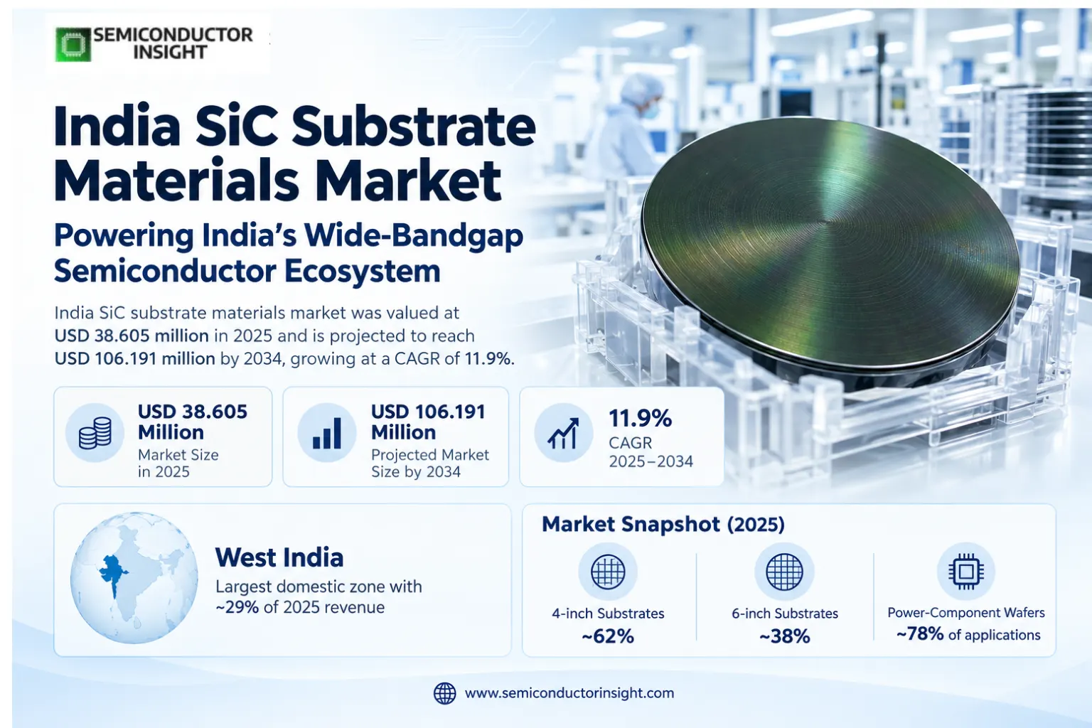
India SiC substrate materials market was valued at USD 38.605 million in 2025 and is projected to reach USD 106.191 million by 2034, growing at a CAGR of 11.9% across the 2025–2034 forecast window. West India represents the largest domestic zone at an estimated ~29% of 2025 revenue, while power-component wafers account for about ~78% of applications. The addressable product is bare SiC crystal substrate material, not the downstream value of completed semiconductors.
Crystalline silicon carbide wafers provide the mechanical and electrical foundation for wide-bandgap power devices that operate under elevated voltage, temperature and switching-frequency conditions. India buys substrates in the 4-inch, equivalent to 100 mm, and 6-inch, equivalent to 150 mm, diameter classes for qualification, epitaxial processing and device fabrication. Material parameters such as 4H polytype, orientation, resistivity, thickness, surface roughness and dislocation density influence whether an epitaxial layer can be grown economically. These requirements make a substrate a qualified manufacturing input rather than a fungible industrial ceramic sheet.
The Indian revenue boundary comprises bare single-crystal SiC substrate materials entering domestic electronics and power-semiconductor programmes, whether supplied by overseas producers or any qualified domestic producer. Separately invoiced epitaxial deposition, finished SiC MOSFETs and diodes, packaging services, conventional silicon wafers and gallium nitride components fall outside this market. This separation is essential because a fabrication project may announce device or wafer-processing capacity without establishing its own boule-growth and wafer-slicing operation. Substrate imports and local processing can coexist within the same Indian manufacturing programme.
Government approval in August 2025 of a SiCSem compound-semiconductor facility in Bhubaneswar provided a significant demand-side signal for the material ecosystem. The project description identifies capacity of 60,000 wafers per year and 96 million packaged units annually, but those are planned fabrication and packaging capabilities, not evidence of 60,000 domestically grown SiC crystals. RIR Power Electronics separately disclosed fiscal support for its Odisha SiC device manufacturing plans. Together these projects can stimulate material qualification, technical service and inventory commitments while retaining dependence on proven substrate supply chains.
India’s industrial purchasing economics are shaped by the trade-off between 100 mm and 150 mm wafers. A 150 mm circular wafer has 2.25 times the nominal surface area of a 100 mm wafer, before edge exclusion, defect losses and device layout effects. The larger format therefore improves the theoretical die opportunity, but conversion requires matched epitaxy reactors, implant and anneal recipes, metrology and reliability data. Suppliers offering both sizes can serve pilot lines without forcing customers into a premature 200 mm migration, which is already advancing in larger overseas fabs.
Demand does not rise uniformly across the five domestic zones. Gujarat and Maharashtra support industrial electronics and logistics; Karnataka and Tamil Nadu provide design and automotive engineering depth; Odisha anchors emerging SiC fab commitments; Punjab has an operating downstream power-device packaging line; and central or northeastern locations mainly contribute engineering, energy and institutional demand. The modeled regional shares reflect these different purchasing channels rather than asserting five separate Indian crystal-growth industries. Long-term growth depends on wafer qualification, not merely the number of announced factories.
Segment Analysis: By Type
4-inch SiC substrate materials lead at an estimated ~62% of 2025 revenue, supported by installed equipment and lower entry cost for pilot manufacturing, while 6-inch substrates account for ~38% and are expected to expand at about ~14.5% CAGR. The 100 mm to 150 mm migration changes usable die area, defect-screening economics and the scope of device qualification. Both sizes remain relevant to Indian customers at different production stages.
| Substrate diameter | Technical and commercial function | Market position |
|---|---|---|
| 4-inch Substrate Materials | The 100 mm diameter enables process-development wafers, lower-volume device programmes and qualification lots where existing deposition and measurement tools remain calibrated for smaller formats. Buyers inspect surface morphology, 4H polytype consistency, off-axis cut, wafer bow and substrate resistivity before committing epitaxy capacity. The smaller format is particularly suitable for engineering organisations that cannot yet amortise a larger-diameter manufacturing line. | Largest type at an estimated ~62% of 2025 material revenue, with modeled ~10.0% CAGR through 2034. The segment benefits from legacy compatibility and faster engineering procurement, although each wafer offers only 44% of the nominal area of a 150 mm wafer. Continued demand is expected in R&D and specialty devices, while new high-throughput fabs favour a gradual diameter transition. |
| 6-inch Substrate Materials | The 150 mm diameter increases nominal circular area by 125% relative to 100 mm and supports greater die output when defect density, edge exclusion and processing yield are controlled. Qualification requires more stringent crystal uniformity across the radius, compatible epitaxial chambers and repeatable metrology. A material supplier must also demonstrate stable wafer thickness and bow across multiple lots, not just a single sample wafer. | Second-largest type at an estimated ~38% share in 2025 and the faster-growing format at ~14.5% CAGR. Rising interest from automotive power devices and industrial conversion favours 150 mm wafer adoption, while capital costs and process learning slow the transition. Commercial buyers may run both 100 mm and 150 mm programmes concurrently until downstream process yields justify an equipment change. |
4-inch wafers: process stability before scale
At 100 mm, buyers can run electrical and materials experiments with relatively contained substrate spending, which matters for Indian laboratories establishing SiC process windows. Typical acceptance procedures compare thickness variation, crystal orientation, micropipes, basal-plane dislocations and polishing quality across more than 1 sample lot. A reliable 4-inch supply contract therefore supports a progression from device concept to small pilot production, even where future 6-inch capacity is contemplated. The near-term market implication is recurring demand for tightly specified small lots rather than an immediate displacement by 200 mm formats.
The commercial strength of this category comes from existing tool compatibility. A development team using 100 mm reactors avoids simultaneous changes to substrate diameter, chamber hardware and thermal recipes, reducing the number of variables that can explain a failed run. Customers still negotiate defect-screening protocols, replacement rights and traceability for each lot. For Indian suppliers and distributors, technical documentation and predictable import lead times may matter as much as the quoted price per wafer, particularly for 2025–2027 qualification campaigns.
6-inch wafers: industrialisation and yield learning
A 150 mm SiC substrate becomes attractive when a customer can spread fixed deposition, lithography and metrology costs over a larger number of devices. The material is not automatically cheaper per good die: crystal defects, epi defects, handling damage and unused edge area can offset the geometric gain. Indian fabs evaluating 6-inch lines consequently require trial lots, statistically useful defect maps and comparable reliability tests. The projected faster growth of this format reflects its manufacturing leverage once those requirements are satisfied.
International suppliers already market 150 mm and 200 mm SiC platforms, but India’s current modeled product classes stop at 6 inches. Infineon and Wolfspeed renewed their 150 mm supply relationship in January 2024, later extending it to 200 mm in October 2026. Those agreements demonstrate that long-term substrate sourcing is a strategic issue for established fabs. Indian entrants can draw lessons from this qualification discipline without counting overseas 200 mm volumes as Indian 6-inch revenue.
Segment Analysis: By Application
Power components account for an estimated ~78% of 2025 substrate material demand, as SiC devices address high-efficiency switching in traction drives, industrial power supplies, renewable generation and charging. RF devices account for ~15% and other specialised uses for ~7%. Each application has distinct resistivity and defect requirements, making a common SiC crystal chemistry insufficient to guarantee interchangeability between power and RF customers.
| Application | Demand characteristics |
|---|---|
| Power Component | Largest application at ~78% share in 2025, growing at a modeled ~12.2% CAGR. Conductive 4H-SiC substrates are evaluated for MOSFETs and Schottky diodes serving electric vehicles, industrial motor drives, high-voltage DC conversion and photovoltaic inverters. The purchasing process combines epitaxial yield, switching reliability, device packaging and multiyear supply guarantees. A wafer that passes dimensional inspection may still be rejected after device-level stress testing, so commercial acceptance extends well beyond raw substrate delivery. |
| RF Device | An estimated ~15% of 2025 material value, with modeled ~11.1% CAGR, serves high-frequency semiconductor structures that may demand different substrate resistivity and defect characteristics from conductive power wafers. Telecom and defence equipment suppliers evaluate thermal conductivity, radio-frequency loss and device linearity, while domestic volumes remain smaller than those for power electronics. Qualification tends to be application-specific and can involve research institutions and international technology partners rather than broad distribution through standard industrial channels. |
| Others | The remaining estimated ~7% of 2025 spending, expanding at ~10.1% CAGR, includes research substrates, material-characterisation programmes and specialised semiconductor experiments not captured by the power or RF categories. University and institutional purchases can involve only a few wafers at a time, but the specifications may be demanding because experimental reproducibility matters. The segment provides an early signal of emerging device architectures without implying that every research demonstration becomes commercial semiconductor production. |
The power-versus-RF split is a technical boundary as well as a sales classification. Conductive SiC wafers can underpin vertical power devices, whereas semi-insulating material may be preferred for certain RF architectures; resistivity requirements are not interchangeable. Suppliers therefore need separate product documentation, customer acceptance limits and traceable crystal lots for different uses. The estimated power-component dominance also means that EV and industrial converter design cycles can influence substrate ordering more than national telecommunications capex alone.
Application diversification reduces concentration but complicates inventory. A distributor stocking 100 mm research material cannot assume that the same wafer grade will satisfy a 150 mm power-device pilot line or a high-frequency customer. Procurement teams review polytype, orientation, wafer thickness, polish finish and defect certification before discussing commercial terms. India’s gradual device-manufacturing expansion favours vendors able to offer engineering consultation and sample-to-production continuity rather than those quoting an undifferentiated price per square centimetre.
Regional Analysis
West India accounts for an estimated ~29% of the India SiC substrate materials market in 2025, followed by South India at ~25% and East India at ~23%. North India contributes ~17%, while Central and Northeast India represent ~6%. East India has the highest modeled growth at ~13.7% CAGR as Odisha progresses SiC device fabrication. The zones describe Indian material demand and procurement influence, not independently verified SiC crystal-growth capacity in each location.
How do five Indian zones differ in bare SiC substrate procurement and qualification?
Geography in this market is determined by where wafer specifications are written, where processing equipment is installed and where materials are delivered, not by a simple count of electronics factories. The western cluster has a broad industrial customer base, the south has substantial design and automotive engineering depth, the east is exposed to new SiC fab investments, the north contributes power-device packaging and design, and central or northeastern locations are more research-oriented. All five zones can use imported 100 mm and 150 mm material even without domestic bulk crystal production.
The five-zone model also separates present spending from future project capacity. Odisha’s SiCSem plans and RIR project support could shift orders toward the east as facilities qualify epitaxy and device processes, whereas West India remains a large buyer through industrial electronics and procurement networks. A faster projected regional CAGR does not guarantee the fastest near-term material shipments; factory commissioning, sample acceptance and stable defect density determine when planned demand becomes actual purchasing. Suppliers that track these milestones can allocate application engineers more efficiently.
| Region | Position | Growth outlook | Demand profile | What decides supplier selection |
|---|---|---|---|---|
| West India | Estimated ~29% of 2025 value | ~10.7% CAGR, 2025–2034 | About USD 11.20 million modeled 2025 material demand; roughly USD 27.95 million implied for 2034 | Supplier traceability, imported wafer availability and converter qualification |
| South India | Estimated ~25% of 2025 value | ~12.7% CAGR, 2025–2034 | About USD 9.65 million modeled 2025 material demand; roughly USD 28.31 million implied for 2034 | Engineering qualification, 150 mm roadmap and automotive-grade reliability |
| East India | Estimated ~23% of 2025 value | ~13.7% CAGR, 2025–2034 | About USD 8.88 million modeled 2025 material demand; roughly USD 28.20 million implied for 2034 | Odisha fab commissioning, 4H-SiC quality and project-stage risk |
| North India | Estimated ~17% of 2025 value | ~10.4% CAGR, 2025–2034 | About USD 6.56 million modeled 2025 material demand; roughly USD 15.99 million implied for 2034 | Device packaging links, lab qualification and supply-chain traceability |
| Central & Northeast India | Estimated ~6% of 2025 value | ~10.6% CAGR, 2025–2034 | About USD 2.32 million modeled 2025 material demand; roughly USD 5.75 million implied for 2034 | Specialist distribution, institutional budgets and import logistics |
Competitive Landscape and Supplier Qualification
The competitive field is led by established international silicon carbide crystal and wafer-material producers, while Indian project developers and downstream device manufacturers influence future demand. Wolfspeed and Coherent provide documented SiC substrate products; Infineon is a major substrate purchaser and power-device manufacturer, not an independent bare-wafer supplier in this Indian model. SiCSem, RIR Power Electronics and CDIL are important domestic ecosystem participants whose reported fabrication or packaging milestones must not be confused with proven commercial bulk crystal growth.
Materials leadership depends on crystal quality, production repeatability and the capacity to supply wafer lots that remain within specification across many manufacturing cycles. Wolfspeed markets 100 mm, 150 mm and 200 mm SiC materials, while Coherent supplies SiC substrates and epitaxial wafer products. Their global portfolios illustrate the demanding level of documentation that Indian buyers encounter when they qualify a new supplier. A competitive bid normally includes defect-density maps, surface specifications, traceability, technical support and a credible multiyear allocation plan.
The transition from 4-inch to 6-inch formats is not simply a pricing exercise. Larger wafers raise the amount of usable material per crystal slice, but yield can be undermined by bow, total thickness variation, scratches, micropipes and basal-plane defects. Indian customers undertaking device process qualification may therefore prefer a supplier with consistent 100 mm lots before scaling to 150 mm. The ability to investigate failed epitaxy runs and replace defective wafers can matter more than a modest difference in quoted unit price.
Several organisations prominent in India’s semiconductor news should be classified by their actual roles. SiCSem has an approved Odisha compound-semiconductor fabrication plan; RIR is developing SiC power-device capability; CDIL commenced high-power device packaging production in Mohali in September 2026. None of these announcements, on its own, verifies high-volume domestic manufacture of SiC substrate boules. Their relevance lies in possible wafer purchasing, qualification and downstream processing rather than established merchant crystal-material market share.
Long-term procurement relationships can favour international suppliers with both 150 mm experience and 200 mm development capability. In January 2024 Wolfspeed and Infineon extended a multiyear 150 mm supply arrangement, and in October 2026 the companies added 200 mm supply. These contracts are international, not Indian substrate revenue, but they reveal how wafer qualification and capacity reservation affect competitive positioning. Indian entrants must decide whether to import proven substrates, partner for technology or build a capital-intensive crystal-growth and polishing operation.
Tier structure
| Tier | Companies | Basis of competition |
|---|---|---|
| Established SiC materials producers | Wolfspeed; Coherent | Documented commercial SiC substrate portfolios and supply relationships form the core direct-supplier tier. These companies can offer specifications for 100 mm and 150 mm material, as well as larger formats outside the defined Indian diameter categories. Buyers evaluate defect certification, wafer flatness, orientation and repeatable lots rather than inferring material share from unrelated corporate revenue. |
| Downstream device and wafer buyers | Infineon Technologies; CDIL Semiconductors | Power-device manufacturers and semiconductor packaging firms influence SiC wafer specifications but should not be automatically classified as merchant substrate suppliers. Infineon’s 150 mm and 200 mm procurement illustrates long-term sourcing discipline; CDIL’s Mohali line manufactures packaged high-power devices. Their presence supports demand-side analysis without attributing bare crystal sales to completed power products. |
| India project and ecosystem participants | SiCSem; RIR Power Electronics; India Semiconductor Mission | Approved SiC device fabrication, investment support and technical ecosystem development may create future substrate qualification demand. The project-stage tier includes organisations whose activities are relevant to material sourcing, engineering and potential future processing capacity. It is not a ranking of verified Indian bulk crystal growers, and announcements must be assessed against actual equipment commissioning and wafer output. |
Key companies profiled
- Wolfspeed, Inc.
- Coherent Corp.
- Infineon Technologies AG
- SiCSem Private Limited
- RIR Power Electronics Limited
- Continental Device India Limited (CDIL)
- India Semiconductor Mission / MeitY
SiC Substrate Production Capacity and Indian Supply Position
India’s immediate SiC substrate opportunity is primarily a material qualification and supply-chain market, rather than a documented nationwide base of high-volume 4H-SiC crystal-growth plants. The 2025 model distinguishes imported 100 mm and 150 mm wafers from domestic wafer processing and device packaging. Announced Indian fab capacity, global 200 mm manufacturing and new high-voltage epitaxy programmes are relevant indicators, but none is a direct count of locally grown 4-inch or 6-inch substrate wafers.
The manufacturing chain begins with high-purity SiC source material and physical-vapour-transport crystal growth, followed by boule inspection, slicing, lapping, polishing and detailed defect mapping. The finished bare substrate then moves to epitaxial deposition before device fabrication. Each stage has a separate yield and cost structure, and a single device fab may import the substrate rather than produce the crystal itself. India’s planned 60,000-wafer SiCSem fabrication capacity therefore cannot be used as an annual estimate of domestic SiC boule or bare-substrate output.
International scale-up provides an important benchmark for India’s sourcing strategy. Coherent announced 200 mm SiC epitaxial wafer shipments in September 2024, and Infineon disclosed 200 mm product rollout in February 2025. Wolfspeed and Infineon subsequently extended their 150 mm wafer supply relationship to 200 mm in October 2026. These steps signal where leading global device makers are investing, but India’s current title-specific product segmentation remains 100 mm and 150 mm bare substrates, not 200 mm or 300 mm heat-spreader materials.
Domestic capacity development is likely to proceed through imported wafer qualification, epitaxial processing, device fabrication and packaging before any broad crystal-material independence is achieved. RIR’s Odisha programme targets high-power SiC devices, while CDIL’s September 2026 Mohali announcement concerns commercial packaging of power semiconductors. Both are relevant demand-side milestones; neither confirms a commercial domestic SiC crystal-boule line. For material suppliers, the near-term production question is whether Indian customers can qualify stable wafers and place repeat orders at the required quality level.
Market Dynamics: Growth Drivers, Restraints and Opportunities
India’s SiC substrate material demand is projected to rise from USD 38.605 million to USD 106.191 million at a 11.9% CAGR, with power-electronics localisation, 150 mm migration and high-voltage device engineering creating the strongest positive forces. Qualification costs, defect-related yield losses and uncertain commissioning schedules temper the outlook. The following impact estimates allocate the forecast growth to commercially distinct forces without treating downstream device announcements as equivalent to substrate shipments.
MARKET DRIVERS
Drivers Impact Analysis*
| Market Drivers | Impact Rank | CAGR Contribution (%) | 2026–2028 | 2029–2031 | 2032–2034 |
|---|---|---|---|---|---|
| Local power-semiconductor fabrication and procurement | High | +4.40% | High | High | Medium |
| EV traction and charging power electronics | High | +3.80% | High | High | High |
| Transition from 100 mm to 150 mm wafer qualification | Medium-High | +3.20% | Medium | High | High |
| Industrial renewable-energy conversion systems | Medium | +2.40% | Medium | High | High |
| Long-term international SiC substrate sourcing | Low-Medium | +1.90% | Medium | Medium | High |
| Others (RF research, institutional material trials, defence electronics) | Low | +1.40% | Low | Medium | Medium |
Domestic SiC fab investment creates a qualification pipeline
The August 2025 approval of the SiCSem compound-semiconductor project in Odisha creates a defined path for future material demand, with government documentation identifying 60,000 wafers per year of planned fabrication capacity and 96 million packaged units. Material suppliers should not book those figures as present substrate sales. The opportunity develops through sample acceptance, epitaxy process establishment and recurring wafer purchasing, which can raise Indian material value over 2026–2034 as projects become operational.
Electrified mobility rewards lower switching losses
Traction inverters and fast chargers can benefit from SiC MOSFETs because high-voltage switching efficiency reduces cooling and passive-component requirements. For the substrate supplier, however, the commercial transaction occurs upstream of a finished charger or vehicle. A buyer first needs 4H-SiC wafers with suitable resistivity, low defect density and reliable orientation. The estimated ~78% power-component share indicates why EV-related engineering has a larger effect on substrate procurement than isolated laboratory RF programmes.
The 150 mm shift expands die opportunity
A 6-inch wafer offers 2.25 times the nominal circular area of a 4-inch wafer, providing a route to more die per process run when defect density and equipment utilisation are controlled. This advantage supports the modeled ~14.5% growth of 6-inch material against ~10.0% for 4-inch. Indian customers still need 150 mm-compatible reactors, wafer handlers and metrology, so the conversion is expected to be gradual rather than an abrupt replacement of qualified 100 mm lines.
Industrial energy systems broaden the demand base
Solar inverters, grid equipment, motor drives and high-voltage power supplies diversify the potential use of SiC devices beyond passenger vehicles. A project may require voltage classes from hundreds of volts to several kilovolts, changing the acceptable defect density and epitaxial structure. Suppliers with consistent 100 mm and 150 mm substrate lots can support different device programmes without attributing the entire downstream system value to the wafer. This diversity can stabilise material ordering through industrial investment cycles.
MARKET RESTRAINTS
Restraints Impact Analysis*
| Market Restraints | Impact Rank | CAGR Contribution (%) | 2026–2028 | 2029–2031 | 2032–2034 |
|---|---|---|---|---|---|
| Crystal defect and epitaxy yield sensitivity | High | -2.20% | High | High | Medium |
| Capital-intensive domestic substrate growth and finishing | Medium-High | -1.40% | High | High | Medium |
| Dependence on imported qualified wafer lots | Medium | -1.00% | High | Medium | Medium |
| Others (commissioning delays, demand timing and logistics) | Low | -0.60% | Medium | Medium | Low |
Material defects amplify downstream costs
Micropipes, dislocations, inclusions and polishing damage can reduce usable die yield after epitaxy and device processing. A substrate that appears acceptable at incoming inspection may create losses after several costly fabrication steps, making quality assurance a central commercial hurdle. Buyers therefore request defect maps, batch traceability and repeat qualification before awarding recurring 150 mm orders. This constraint is particularly severe for Indian projects seeking automotive or high-voltage reliability rather than laboratory-only performance.
Crystal-growth capacity requires specialised investment
Building a domestic SiC boule-growth and wafer-finishing operation is different from establishing a semiconductor packaging line. It requires high-temperature crystal growth, slicing, polishing, metrology and a stable process capable of controlling defects over many runs. Announced device fabs and epitaxial installations may source wafers externally. The capital and learning-curve burden can delay local substrate substitution even when government-supported downstream power semiconductor programmes are progressing.
Import dependence creates planning exposure
Qualified bare wafers may travel through international procurement, export documentation and logistics channels before reaching Indian device developers. A delayed 100 mm research lot or 150 mm production trial can postpone epitaxy experiments and reliability validation. Long-term agreements such as the Wolfspeed–Infineon 150 mm arrangement illustrate why leading fabs reserve material capacity. Indian buyers without similar purchasing scale may face longer lead times or less flexible lot allocation during periods of global demand pressure.
MARKET OPPORTUNITIES
Material characterisation services near device projects
Indian projects can develop local value without immediately operating a bulk crystal-growth plant by offering incoming wafer inspection, defect mapping, traceability and supplier-qualification services. Such work is relevant to 100 mm research lots and 150 mm process-development lots, particularly where epitaxy and device fabrication are being established. A service partner that links substrate maps to device yield data can reduce customer qualification cycles and become embedded in recurring procurement decisions.
Supply agreements tailored to domestic fab milestones
An international SiC substrate producer can enter India through staged commitments tied to customer equipment acceptance rather than promising full commercial volume at project approval. Early contracts may specify 4-inch sample lots, followed by 6-inch pilot wafers and optional production allocation after process yield targets are reached. This structure protects both supplier capacity and customer working capital while creating a credible path from India’s semiconductor investment announcements to actual material orders.
Specialised RF and high-voltage material grades
Although power devices dominate modeled revenue, RF and advanced industrial applications create opportunities for grades with distinct resistivity, thickness and defect specifications. A research customer evaluating semi-insulating SiC for RF may have little overlap with a conductive substrate used for a power MOSFET. Suppliers that can document both material families can build a technically differentiated position in India rather than competing solely on the price of standard 4H-SiC wafer lots.
Value Chain, Sourcing and Commercial Access
The SiC materials value chain runs from high-purity source preparation and crystal-boule growth through slicing, polishing, substrate qualification, epitaxy and device fabrication. Indian demand currently spans engineering samples, imported qualified wafers and planned downstream semiconductor processing. A reliable procurement pathway requires agreement on wafer diameter, crystal orientation, resistivity, defect acceptance and responsibility for failed lots before customers can establish recurring substrate orders.
Upstream crystal control. A substrate manufacturer’s competitive advantage begins before the wafer is cut. Temperature distribution during boule growth, 4H polytype stability and defect propagation determine the material that later reaches an Indian fab. Surface polishing cannot remove every bulk crystal defect, so procurement specifications must cover both subsurface and surface characteristics. A supplier able to link 100 mm and 150 mm lot history to device yield can command stronger customer confidence than a reseller with only a dimensional datasheet.
Midstream qualification. India-based laboratories and device developers often need wafer characterisation before they can choose an epitaxy recipe. Incoming inspection can include total thickness variation, bow, warp, orientation, micropipes and basal-plane dislocation mapping, followed by trial epitaxy and electrical test structures. The work may span several rounds over 2025–2027, particularly for automotive or high-voltage applications. Successful qualification makes a material vendor difficult to replace because switching suppliers can force renewed reliability testing.
Downstream value separation. A SiC wafer used in a MOSFET eventually becomes part of a power module, charger or inverter, but each step creates additional value. The material market counts the bare substrate transaction rather than the revenue of finished devices or electric vehicles. This distinction matters when interpreting announcements of 60,000 planned fabrication wafers or 96 million packaged units: those figures do not establish either wafer material selling prices or the amount of Indian-grown SiC crystal output.
Commercial route to market. The most practical entry strategy combines application engineering, local inventory support and direct relationships with planned semiconductor fabrication projects. Customers may begin with a 100 mm specification and transition to 150 mm after equipment and yield reviews. Contract terms should address sample replacement, traceability, shipment conditions, process changes and allocation during global shortages. These provisions can determine whether a supplier becomes a repeat vendor rather than a one-time source of laboratory wafers.
Recent Developments Affecting SiC Substrate Sourcing
- 15 October 2026 Direct material sourcing
Wolfspeed and Infineon expanded their long-term silicon carbide wafer supply relationship to include 200 mm material alongside the existing 150 mm arrangement. The announcement is a global supplier qualification and capacity-reservation signal, not an Indian 200 mm substrate shipment. It matters to Indian 4-inch and 6-inch buyers because leading device manufacturers continue to secure wafer quality and long-term supply well before committing production programmes to a larger diameter. Source - 17 September 2026 Adjacent India device manufacturing
CDIL announced commercial operation of a new Mohali assembly, testing, marking and packaging line for high-power semiconductor devices, including silicon carbide products. This establishes a concrete downstream manufacturing milestone in North India, but the line does not prove that CDIL grows SiC crystal boules or sells bare substrates. Its relevance is the possible strengthening of domestic device demand, technical skills and future material qualification relationships around Indian power electronics. Source - 9 April 2026 Adjacent epitaxy technology
Coherent disclosed thick SiC epitaxy capabilities for 150 mm and 200 mm platforms supporting device architectures up to 10 kV. The development concerns epitaxial processing and high-voltage device requirements, not direct sales of 4-inch or 6-inch bare wafers in India. It nevertheless illustrates why crystal defect control and substrate uniformity matter: thicker epitaxial structures make material imperfections more consequential to manufacturing yield and final device reliability. Source - 15 August 2025 India semiconductor policy
India’s Press Information Bureau summarised the semiconductor project pipeline, identifying the SiCSem Bhubaneswar compound-semiconductor proposal with 60,000 planned fabrication wafers per year and 96 million units of packaging capacity. The document strengthens the evidence for a domestic SiC device-processing pipeline, while the capacity numbers must not be recast as verified Indian crystal-substrate production. Material demand will depend on actual tool installation, wafer qualification and repeat purchasing after project commissioning. Source - 7 August 2025 Adjacent Odisha project
RIR Power Electronics reported Odisha fiscal support for its Bhubaneswar SiC semiconductor manufacturing facility. The proposed high-power device programme covers voltage requirements from 3.3 kV to 20 kV, creating a potential need for carefully qualified substrate and epitaxial material. The announcement is an investment and development milestone rather than evidence of commercial SiC boule growth; the material-market effect arises only as device fabrication and procurement milestones are achieved. Source - 13 February 2025 Adjacent global diameter transition
Infineon announced the first customer releases of SiC power products made using its 200 mm wafer technology, with manufacturing activity in Villach and a planned ramp in Kulim. This illustrates the global shift toward larger-diameter production, which can improve die economics when yields are maintained. The development is adjacent to India’s defined 100 mm and 150 mm bare-substrate classes and must not be counted as a domestic 200 mm materials market transaction. Source - 26 September 2024 Direct materials and adjacent epitaxy
Coherent announced 200 mm SiC epitaxial wafer production and stated that substrate and epitaxial wafer shipments were underway. The disclosure demonstrates the technical progression from qualified bare material to larger-diameter epitaxial products in the international supply chain. For India, it is evidence of supplier capability and future technology direction, not proof of local commercial crystal output or revenue from the 4-inch and 6-inch segments modelled here. Source
REPORT SCOPE & SEGMENTATION
| Attribute | Details |
|---|---|
| Market | India SiC Substrate Materials |
| Base year | 2025 |
| Estimate year | 2026 |
| Forecast year | 2034 |
| Currency | USD million |
| Revenue boundary | Bare crystalline SiC substrate materials supplied for Indian device and research use; imported and qualified domestic supply included, separately billed epitaxy and finished devices excluded. |
| By Type | 4-inch Substrate Materials · 6-inch Substrate Materials |
| By Application | Power Component · RF Device · Others |
| By Region | Single-country market: five domestic Indian zones; estimated shares refer to Indian substrate demand, not five independent bulk crystal production centres. West IndiaGujarat · Maharashtra · western industrial and semiconductor procurement South IndiaKarnataka · Tamil Nadu · southern design and automotive electronics East IndiaOdisha · West Bengal · SiC device-fabrication investment corridor North IndiaPunjab · Uttar Pradesh · device packaging and engineering Central & Northeast IndiaMadhya Pradesh · Assam · regional research and emerging electronics |
| Key Companies Profiled | Wolfspeed; Coherent; Infineon Technologies; SiCSem; RIR Power Electronics; Continental Device India Limited; India Semiconductor Mission |
| Customization Scope | Domestic zone allocations, 100 mm and 150 mm material grades, conductive versus semi-insulating specifications, crystal defect acceptance, wafer sourcing routes, device-project milestones, and application-specific qualification schedules. |
Frequently Asked Questions
What is the India SiC substrate materials market size and forecast?
The India SiC substrate materials market is valued at USD 38.605 million in 2025 and is forecast to reach USD 106.191 million by 2034, implying a 11.9% CAGR. The product is bare crystalline silicon carbide wafer material used for subsequent epitaxy and device manufacturing. The forecast does not add completed power-device revenue, separately billed epitaxial deposition or the value of downstream electric vehicles and industrial equipment.
Which SiC wafer diameter holds the largest Indian share?
The 4-inch, or 100 mm, substrate category holds an estimated ~62% of 2025 Indian value, with 6-inch, or 150 mm, material at ~38%. The smaller format benefits from established process tools and pilot activity, whereas 150 mm is modeled to expand faster at ~14.5% CAGR. The larger diameter offers 2.25 times the nominal wafer area, but manufacturing benefit depends on defects, edge exclusion and device yield.
Which Indian zone leads substrate material demand?
West India leads with an estimated ~29% of 2025 value, followed by South India at ~25%, East India at ~23%, North India at ~17% and Central and Northeast India at ~6%. These allocations describe purchasing and qualification influence across India. They do not imply that each zone operates an independent commercial SiC boule-growth facility, and they distinguish existing industrial demand from announced future fabs.
What is the fastest-growing domestic zone?
East India is modeled to expand at ~13.7% CAGR through 2034, ahead of South India at ~12.7%, reflecting Odisha’s SiC device-fabrication project pipeline. The SiCSem proposal has a stated annual fabrication capacity of 60,000 wafers, but that is not a verified output of bare SiC crystals. Actual material orders will depend on commissioning, epitaxial qualification and customer acceptance of wafer quality.
Which applications consume the most SiC substrate material?
Power components account for an estimated ~78% of 2025 Indian material spending, compared with ~15% for RF devices and ~7% for other uses. Power demand is connected to traction inverters, charging, industrial motor drives and renewable-energy conversion. RF material can require a different resistivity specification, so a conductive power wafer is not necessarily interchangeable with a semi-insulating RF substrate even when both use 4H-SiC.
Does India manufacture all of the SiC substrates it uses?
No. India’s emerging SiC device and semiconductor processing initiatives do not establish that every substrate is domestically grown. The market includes imported, qualified bare wafers, while projects in Odisha and packaging activity in Mohali demonstrate different stages of the semiconductor chain. Crystal-boule growth, slicing, polishing, epitaxy, device fabrication and packaging should be tracked separately when evaluating domestic content or import dependence.
How are 4-inch and 6-inch SiC substrates commercially different?
A 6-inch wafer has 150 mm nominal diameter and 2.25 times the circular area of a 100 mm, 4-inch wafer. That can improve the number of devices per run, but only if epitaxial uniformity, defect density and equipment utilisation support acceptable yield. Four-inch material remains useful for pilot qualification, while six-inch material generally requires larger reactors, handling equipment and a longer process-validation cycle.
Which companies are relevant to Indian SiC substrate sourcing?
Wolfspeed and Coherent are documented international SiC material suppliers, and Infineon is a major power-device manufacturer with long-term wafer procurement relationships. In India, SiCSem, RIR Power Electronics and CDIL are important fabrication, development or packaging participants. Their roles should not be conflated: a company manufacturing SiC devices or announcing a fab is not automatically a verified seller of commercial bare crystal substrates.
What determines substrate qualification and supplier selection?
Buyers examine crystal polytype, wafer orientation, resistivity, thickness, bow, total thickness variation, surface damage and defect maps. They also consider the supplier’s ability to deliver consistent 100 mm or 150 mm lots, trace failed wafers and support epitaxial troubleshooting. A material grade suitable for laboratory experiments may not satisfy automotive reliability requirements, so qualification extends into device-level electrical stress and process yield.
How do global 200 mm SiC developments affect this Indian market?
International suppliers are moving toward 200 mm production, as shown by Coherent’s 2024 announcement and the Wolfspeed–Infineon supply expansion in October 2026. These developments can influence future cost expectations, equipment planning and long-term wafer sourcing. They do not change the defined Indian market segmentation of 4-inch and 6-inch bare substrates or establish that 200 mm wafers are being produced commercially in India.
Research Sources & Evidence Base

Get Sample Report PDF for Exclusive Insights
Report Sample Includes
- Table of Contents
- List of Tables & Figures
- Charts, Research Methodology, and more...
 Download Sample Report PDF